
Electrostatic Discharge Protection Structure

An electrostatic discharge protection and voltage technology, applied in circuits, electrical components, electric solid devices, etc., can solve the problems of high discharge current, reduce electrostatic protection, burnout, etc., and achieve the effect of improving conduction uniformity and electrostatic discharge capacity.

Active Publication Date: 2016-12-28
SEMICON MFG INT (SHANGHAI) CORP
View PDF3 Cites 0 Cited by
  • Summary
  • Abstract
  • Description
  • Claims
  • Application Information

AI Technical Summary

Problems solved by technology

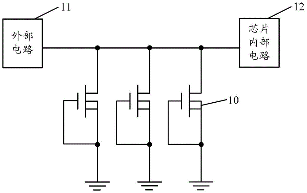
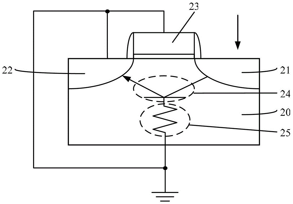
However, due to layout design considerations, the existing ground connection area is generally located at the outermost side of the GGNMOS transistor, so that the parasitic resistances corresponding to different positions of the GGNMOS transistor in the prior art are different, so that the source and the substrate are close to the source and drain. The potential difference of the pole part is also different, and the parasitic NPN transistors formed by the source, substrate, and drain will not be turned on at the same time, so that the conduction uniformity of multiple GGNMOS transistors in the existing electrostatic discharge protection circuit is poor.
When some of the GGNMOS transistors are turned on, the others are not easy to turn on, which will seriously affect the ability of the electrostatic discharge protection circuit, which may cause the discharge current to be too high and burn out. Passing the GGNMOS transistor will not be able to play a protective role, reducing the ability of electrostatic protection

Method used


Image

  • Electrostatic Discharge Protection Structure
  • Electrostatic Discharge Protection Structure
  • Electrostatic Discharge Protection Structure

Examples


Embodiment Construction

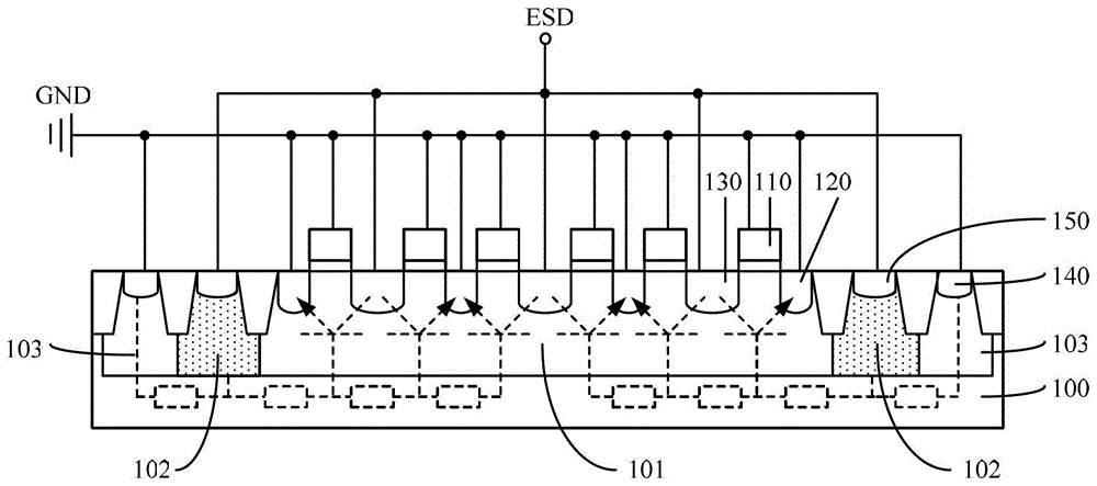
[0031] Since multiple GGNMOS transistors formed in the prior art cannot be turned on at the same time, and the conduction uniformity is poor, an embodiment of the present invention provides an electrostatic discharge protection structure, which specifically includes: a P-type semiconductor substrate; Several NMOS transistors arranged side by side on the surface of the P-type semiconductor substrate are located in the connection region and the N-type well region in the P-type semiconductor substrate, and the N-type well region is at least located between the connection region and the NMOS transistors; The N-type well region and the drain of the NMOS transistor are connected to the electrostatic discharge input terminal, and the source of the NMOS transistor is connected to the ground terminal.

[0032]Since the N-type well region is located at least between the connection region and the NMOS transistor, when the electrostatic voltage generated by the external electrostatic pulse...


PUM


Abstract

An electrostatic discharge protection structure, comprising: a P-type semiconductor substrate; a number of NMOS transistors arranged side by side on the surface of the P-type semiconductor substrate, a connection region and an N-type well region located in the P-type semiconductor substrate, the The N-type well region is at least located between the connection region and the NMOS transistor; the drain of the N-type well region and the NMOS transistor is connected to the electrostatic discharge input terminal, and the source of the NMOS transistor is connected to the ground terminal. Since the N-type well region is located at least between the connection region and the NMOS transistor, when the electrostatic voltage generated by the external electrostatic pulse is applied to the electrostatic discharge input terminal, the N-type well region will increase the substrate voltage of the NMOS transistor , so that the source and substrate of the NMOS transistor are easily turned on, which is beneficial to improving the conduction uniformity of the electrostatic discharge protection structure and improving the electrostatic protection capability.

Description

technical field [0001] The invention relates to the field of integrated circuits, in particular to an electrostatic discharge protection structure. Background technique [0002] As semiconductor chips are used more and more widely, the electrostatic damage involved in semiconductor chips is also more and more extensive. There are many designs and applications of electrostatic discharge protection circuits, usually including: gate grounded N-type field effect transistor (Gate Grounded NMOS, GGNMOS) protection circuit, diode protection circuit, silicon controlled rectifier (Silicon ControlledRectifier, SCR) protection circuit, etc. . [0003] Among them, the circuit diagram of the gate grounded N-type field effect transistor (Gate Grounded NMOS, GGNMOS) protection circuit is as follows figure 1 As shown, the multiple gate-grounded N-type field effect transistors 10 are located between the external circuit 11 and the internal circuit 12 of the chip, and the drains of the gate...

Claims


Application Information

Patent Timeline
Patent Type & Authority Patents(China)
IPC IPC(8): H01L27/02
Inventor 甘正浩
Owner SEMICON MFG INT (SHANGHAI) CORP
Learn More