
Electrostatic Discharge Protection Structure

An electrostatic discharge protection and voltage technology, which is applied in the direction of circuits, electrical components, electric solid devices, etc., can solve the problems of low electrostatic discharge capacity and poor electrostatic protection ability, and achieve improved electrostatic discharge capacity, easy conduction, and increased quantity Effect

Active Publication Date: 2017-06-13
SEMICON MFG INT (SHANGHAI) CORP
View PDF5 Cites 0 Cited by
  • Summary
  • Abstract
  • Description
  • Claims
  • Application Information

AI Technical Summary

Problems solved by technology

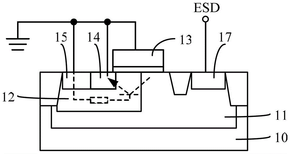
However, the electrostatic discharge protection structure formed by the LDMOS transistor has low electrostatic discharge capability, which makes the electrostatic protection capability poor.

Method used


Image

  • Electrostatic Discharge Protection Structure
  • Electrostatic Discharge Protection Structure
  • Electrostatic Discharge Protection Structure

Examples


Embodiment Construction

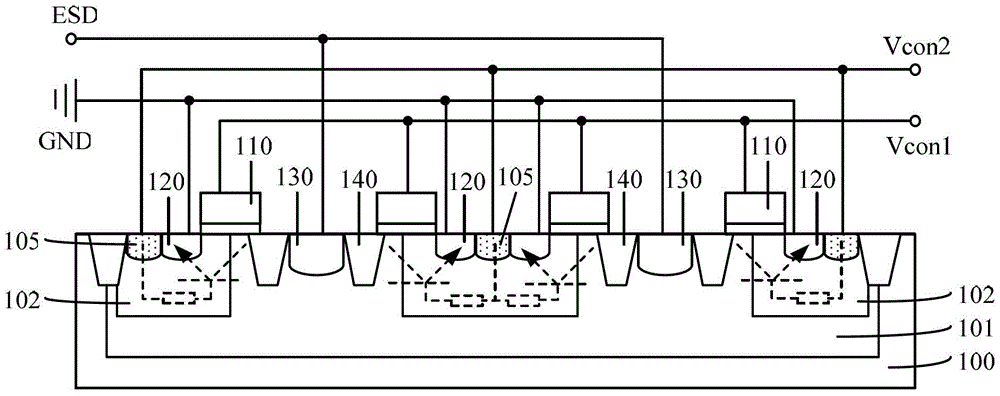
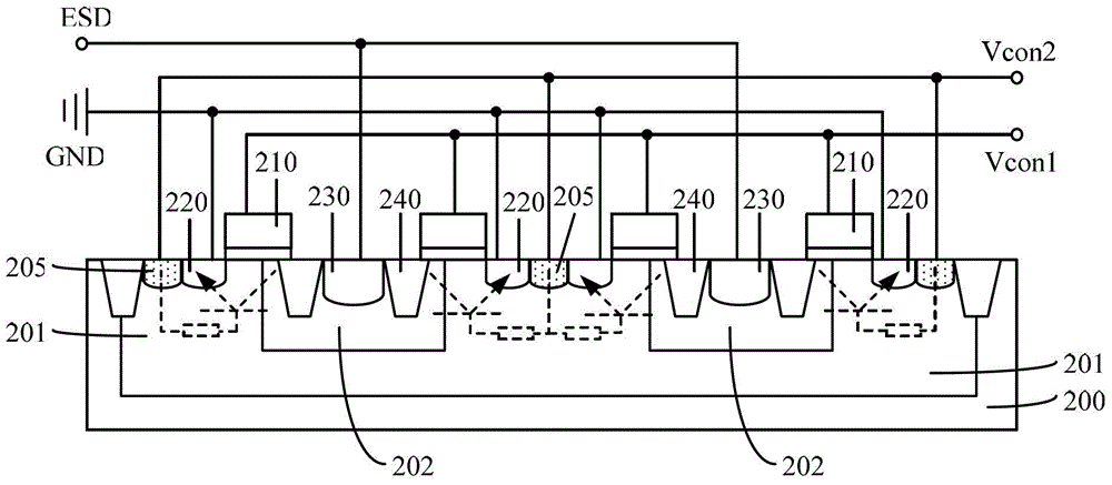
[0027] Since the electrostatic discharge protection structure formed by a single LDMOS transistor has low electrostatic discharge capability and poor electrostatic protection capability, the present invention provides an electrostatic discharge protection structure that connects multiple LDMOS transistors together as an electrostatic discharge protection structure, not only improves the electrostatic discharge capability, and because the potential difference between the source of each LDMOS transistor and the P-type body region close to the source is the same, the LDMOS transistors of the electrostatic discharge protection structure can be turned on at the same time, improving the The conduction uniformity of the electrostatic discharge protection structure and the number of conduction LDMOS transistors improve the electrostatic discharge capability.

[0028] In order to make the above objects, features and advantages of the present invention more comprehensible, specific embod...


PUM


Abstract

An electrostatic discharge protection structure, comprising: a semiconductor substrate; a plurality of N-type lateral diffusion field effect transistors arranged in parallel on the surface of the semiconductor substrate; a P-type body region located in the semiconductor substrate, and a source in the P-type body region Pole, channel region and body region connection region, the body region connection region is located on the outside of each N-type laterally diffused field effect transistor near the source; the drain of each N-type laterally diffused field effect transistor is connected to the electrostatic discharge input terminal , the source of each N-type laterally diffused field-effect transistor is connected to the ground terminal, the gate of each N-type laterally diffused field-effect transistor is connected to the first control voltage terminal, and each body region is connected to the second control voltage terminal. connected to the voltage terminals. A plurality of LDMOS transistors are connected together as an electrostatic discharge protection structure, which not only improves the electrostatic discharge capability, but also enables each parasitic triode to be turned on at the same time, thereby improving the conduction uniformity of the electrostatic discharge protection structure.

Description

technical field [0001] The invention relates to semiconductor technology, in particular to an electrostatic discharge protection structure. Background technique [0002] As semiconductor chips are used more and more widely, the electrostatic damage involved in semiconductor chips is also more and more extensive. There are many designs and applications of electrostatic discharge protection circuits, usually including: gate grounded N-type field effect transistor (Gate Grounded NMOS, GGNMOS) protection circuit, silicon controlled rectifier (SCR) protection circuit, lateral diffusion field Effect transistor (Laterally Diffused MOS, LDMOS) protection circuit, etc. [0003] Please refer to figure 1 , is a structural schematic diagram of an electrostatic discharge protection structure formed by using LDMOS transistors in the prior art, specifically including: a P-type substrate 10, an N-type well region 11 located in the P-type substrate 10, and an N-type well region 11 located ...

Claims


Application Information

Patent Timeline
Patent Type & Authority Patents(China)
IPC IPC(8): H01L27/04H01L23/60
Inventor 甘正浩
Owner SEMICON MFG INT (SHANGHAI) CORP
Learn More