
Anti-fuse circuit, programming method thereof and anti-fuse structure

An anti-fuse and circuit technology, applied in circuits, electrical components, electrical solid devices, etc., can solve problems such as poor stability of polysilicon anti-fuses, and achieve the effects of reducing programming voltage, improving programming speed, and easy to punch through.

Active Publication Date: 2014-10-15
SEMICON MFG INT (SHANGHAI) CORP
View PDF3 Cites 3 Cited by
  • Summary
  • Abstract
  • Description
  • Claims
  • Application Information

AI Technical Summary

Problems solved by technology

[0006] But the stability of the existing polysilicon antifuse is poor

Method used


Image

  • Anti-fuse circuit, programming method thereof and anti-fuse structure
  • Anti-fuse circuit, programming method thereof and anti-fuse structure
  • Anti-fuse circuit, programming method thereof and anti-fuse structure

Examples


Embodiment Construction

[0033] The existing amorphous silicon antifuse is easily affected by metal electromigration characteristics, and the stability of the amorphous silicon antifuse is poor.

[0034] For this reason, the inventor of the present invention proposes a kind of antifuse circuit and antifuse structure, adopts PMOS transistor as antifuse, utilizes the hot carrier punch-through effect of PMOS transistor, makes the source region and drain region of PMOS transistor Punch through to complete the programming of the antifuse, which improves the stability of the antifuse. In addition, the width of the second part of the gate of the PMOS transistor of the present invention is smaller than the width of the first part, so that the width of the channel region (dimensions along the direction of the source region and the drain region) at the edge of the PMOS transistor is reduced. When programming , so that the source region and the drain region of the PMOS transistor are easier to punch through, whi...


PUM

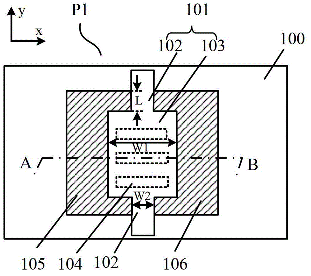
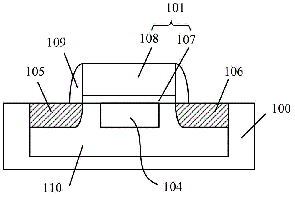

Abstract

The invention relates to an anti-fuse circuit, a programming method thereof and an anti-fuse structure. The anti-fuse structure comprises: a semiconductor substrate and a PMOS transistor positioned on the semiconductor substrate, the grid of the PMOS transistor is positioned on the semiconductor substrate, the grid has a first portion and a second portion positioned at two ends of the first portion, the width of the second portion is less than the width of the first portion, the source region and the drain region of the PMOS transistor are positioned in the semiconductor substrate at two sides of the first portion and the second portion of the grid, and the source region and the drain region of the PMOS transistor break through under the action of a hot carrier break-through effect when the anti-fuse is programmed. The anti-fuse structure has a high stability after programming.

Description

technical field [0001] The invention relates to the field of semiconductors, in particular to an antifuse circuit, a programming method thereof, and an antifuse structure. Background technique [0002] Antifuse (Antifuse) is a very important one-time programmable interconnection unit, which is widely used in the fields of computer, communication, automobile, satellite and aerospace. [0003] Semiconductor devices based on antifuse have very superior performance, which is mainly reflected in the following methods: (1) It is non-volatile, and the antifuse is programmed through the programming voltage, and the antifuse changes from a state after programming It is another state, the change of this state is irreversible, and the changed programming state can be saved permanently; (2) It has radiation resistance, anti-fuse is a natural anti-radiation component, it can not only withstand nuclear (3) High reliability, some studies have shown that the reliability of anti-fuse device...

Claims


Application Information

Patent Timeline
IPC IPC(8): G11C17/16H01L23/525
Inventor 甘正浩
Owner SEMICON MFG INT (SHANGHAI) CORP
Learn More