


Quick Research
Generate reliable direction feasibility study reports for your R&D in just a few steps.

Technical Q&A
Discover and master advanced knowledge NOW. Basics, ideas, possibilities, all at once.

Find Solutions
As an expert in R&D theories, this can generate solutions to your technical problems instantly.

Evaluate Feasibility
Analyze your overall solution with one click, know your potential R&D risks in advance.

Monitor Landscape
Get weekly tech updates, stay abreast of the latest tech innovations and key insights.
Writing method of nonvolatile memory unit array
A technology of memory unit and storage unit, which is applied in the field of integrated circuits, can solve the problems of device upgrading, area reduction, application restriction, etc., and achieve the effect of reducing area and high cost performance
- Summary
- Abstract
- Description
- Claims
- Application Information
AI Technical Summary
Problems solved by technology
Method used
Image

Examples
Embodiment Construction
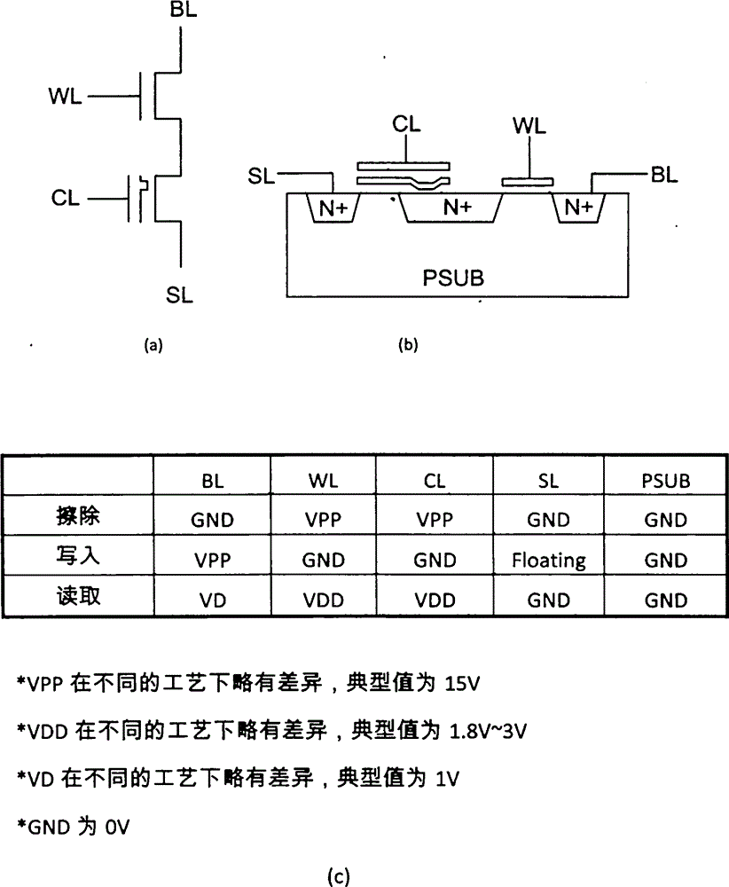
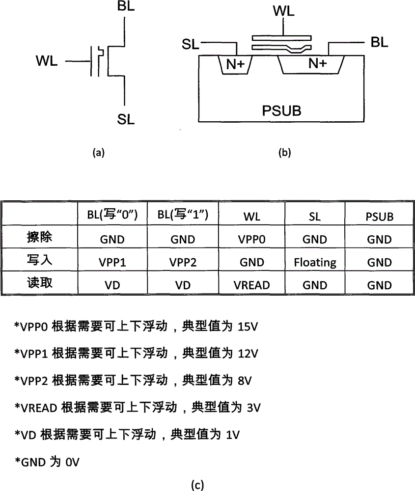
[0011] The writing method of the non-volatile memory cell array of the present invention will be described in detail below with reference to the accompanying drawings.
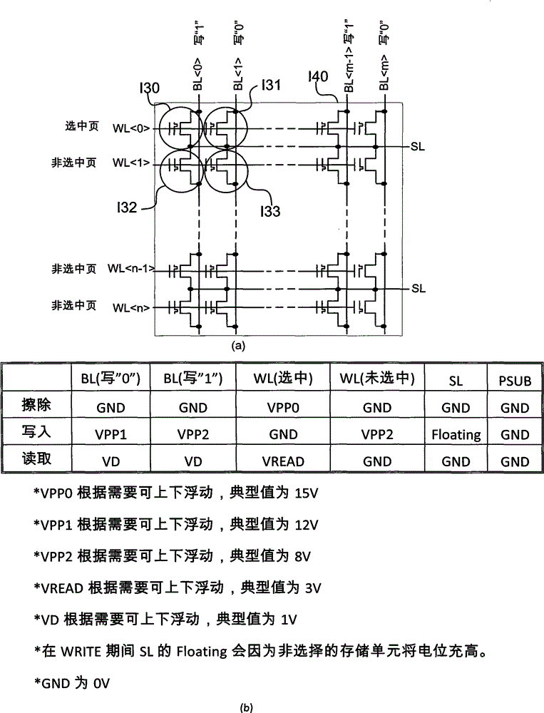
[0012] image 3 It is the non-volatile memory cell array of the present invention, (a) is a schematic diagram, and (b) is the voltage of corresponding terminals during erasing and writing operations. Such as image 3 As shown in (a), I40 in the figure is a memory array with n word lines and m bit lines. In the figure, for example: WL is the selected word line, and even bit lines write logic "0" , the odd bit line writes a logic "1". In this way, there are four types of memory cells in different voltage environments in the entire array, as follows:
[0013] I30: Select the word line, write logic "0" to the bit line
[0014] I31: Select the word line, write logic "1" to the bit line
[0015] I32: unselected word line, bit line write logic "0"
[0016] I33: Unselected word line, bit line write logic "1"
...
PUM
 Abstract
Description
Claims
Application Information
 - R&D Engineer
- R&D Manager
- IP Professional
- Industry Leading Data Capabilities
- Powerful AI technology
- Patent DNA Extraction
Browse by: Latest US Patents, China's latest patents, Technical Efficacy Thesaurus, Application Domain, Technology Topic, Popular Technical Reports.
© 2024 PatSnap. All rights reserved.Legal|Privacy policy|Modern Slavery Act Transparency Statement|Sitemap|About US| Contact US: help@patsnap.com