PCB structure capable of preventing tin connection of adjacent pads

A technology for PCB boards and pads, applied in the field of PCB structure that can prevent adjacent pads from connecting tin, can solve problems such as easy soldering, achieve reliable solder joints, prevent soldering, and low cost

Inactive Publication Date: 2014-10-08
深圳市磊科实业有限公司
View PDF5 Cites 8 Cited by
  • Summary
  • Abstract
  • Description
  • Claims
  • Application Information

AI Technical Summary

Problems solved by technology

[0006] The purpose of the present invention is to provide a PCB board structure that can prevent adjacent pads from connecting tin, and mainly solve the problem that soldering pads in existing PCB boards are prone to soldering.

Method used


Image

  • PCB structure capable of preventing tin connection of adjacent pads
  • PCB structure capable of preventing tin connection of adjacent pads

Examples


Embodiment

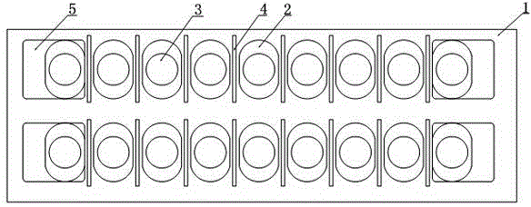
[0023] like figure 2 As shown, the present invention includes a PCB board main body 1 , solder pads 2 and a silk screen white oil layer 4 . The pad 2 is arranged on the PCB board main body 1, and the pad 2 is provided with a solder hole 3 for the insertion of the solder leg of the plug-in component, and the solder pad 2 is penetrated into the solder hole 3 by the solder leg of the plug-in component Finally, the plug-in components are welded to the main body of the PCB board. There are multiple pads 2, and all the pads are arranged in sequence to form a pad group. The direction of the pad arrangement is parallel to the direction of the PCB board going through the furnace. Each pad is in the shape of a racetrack, and two adjacent pads are arranged in such a way that the straight sides of the raceway face face each other, which can effectively increase the distance between adjacent pads and prevent tin connection.

[0024] Further, since two adjacent pads are arranged in a race...


PUM


Abstract

The invention discloses a PCB structure capable of preventing tin connection of adjacent pads, for solving the problem of tin connection easily generated during welding of pads in a PCB. The PCB structure comprises a PCB main body and the N pads which are arranged on the PCB main body and are provided with welding holes. All the pads are sequentially arranged to form a pad group, the pad arrangement direction is parallel to the furnace direction of a PCB, N is a natural number greater than one, the pads are runway-shaped, the adjacent two pads are arranged in such a way that the runway-shaped straight edges are opposite, and the PCB main body area between the adjacent pads is provided with a silkscreen white oil layer whose length is not smaller than the length of the pads; and tin dragging pads connected with the pads at edges are disposed at the two ends of the pad group on the reverse surface of the PCB main body. The design is ingenious, the problem of tin connection between the tail portions of the pads and between the adjacent pads can be effectively solved, the labor cost is saved, and the production efficiency is also substantially improved.

Description

[0001] technical field [0002] The invention relates to a PCB board structure, in particular to a PCB board structure capable of preventing adjacent pads from connecting tin. Background technique [0003] Tin connection means that when soldering components, two or more solder joints are connected together by solder, resulting in poor product function and appearance. Therefore, when soldering components, the phenomenon of tin connection should be avoided as much as possible. [0004] At present, in the process of soldering plug-in components to the PCB board, since the direction of the PCB board through the furnace is the direction of tin falling, the conventional pad design on the PCB board will connect the tin in the middle of the two pads into one piece. like figure 1 As shown, in the conventional pad design, the pads are all circular, so the distance between adjacent pads is small, and the phenomenon of tin connection is very difficult to avoid. During wave solderi...

Claims


Application Information

Patent Timeline
Patent Type & Authority Applications(China)
IPC IPC(8): H05K1/11
Inventor 许薇
Owner 深圳市磊科实业有限公司
Why Eureka
Try Eureka