High-uniformity GaN film growing on sapphire substrate and preparing method and application of high-uniformity GaN film

A sapphire substrate, uniform technology, used in climate sustainability, final product manufacturing, sustainable manufacturing/processing, etc., can solve the problem of high cost, difficulty in preparing high uniformity GaN thin films, and low LED luminous efficiency and other problems, to achieve the effect of improving utilization, repeatability, and unique growth process

Active Publication Date: 2014-08-20
HEYUAN CHOICORE PHOTOELECTRIC TECH CO LTD
View PDF3 Cites 2 Cited by
  • Summary
  • Abstract
  • Description
  • Claims
  • Application Information

AI Technical Summary

Problems solved by technology

The 21st century will be an era of new lighting sources represented by LEDs, but at this stage, LEDs have low luminous efficiency and high cost, which greatly restricts the development of LEDs in the direction of high efficiency, energy saving and environmental protection.
However, due to the small area of ​​the plasma plume generated by the laser, it is difficult to prepare GaN films with high uniformity, which has become one of the limiting conditions for pulsed laser deposition.

Method used


Image

  • High-uniformity GaN film growing on sapphire substrate and preparing method and application of high-uniformity GaN film
  • High-uniformity GaN film growing on sapphire substrate and preparing method and application of high-uniformity GaN film
  • High-uniformity GaN film growing on sapphire substrate and preparing method and application of high-uniformity GaN film

Examples


Embodiment 1

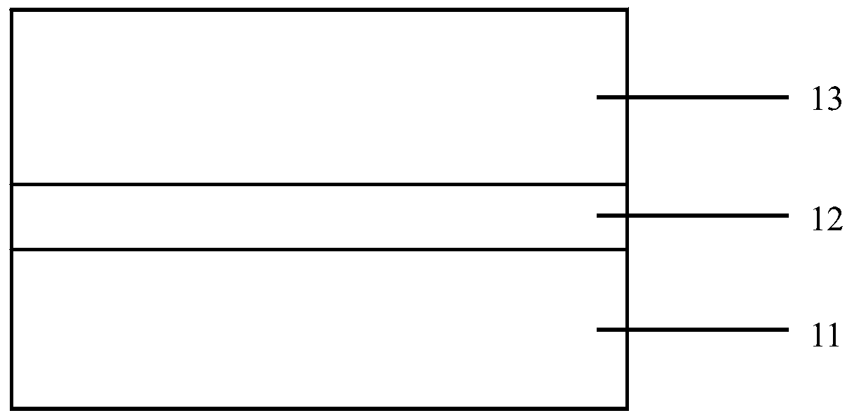
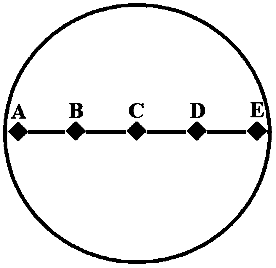
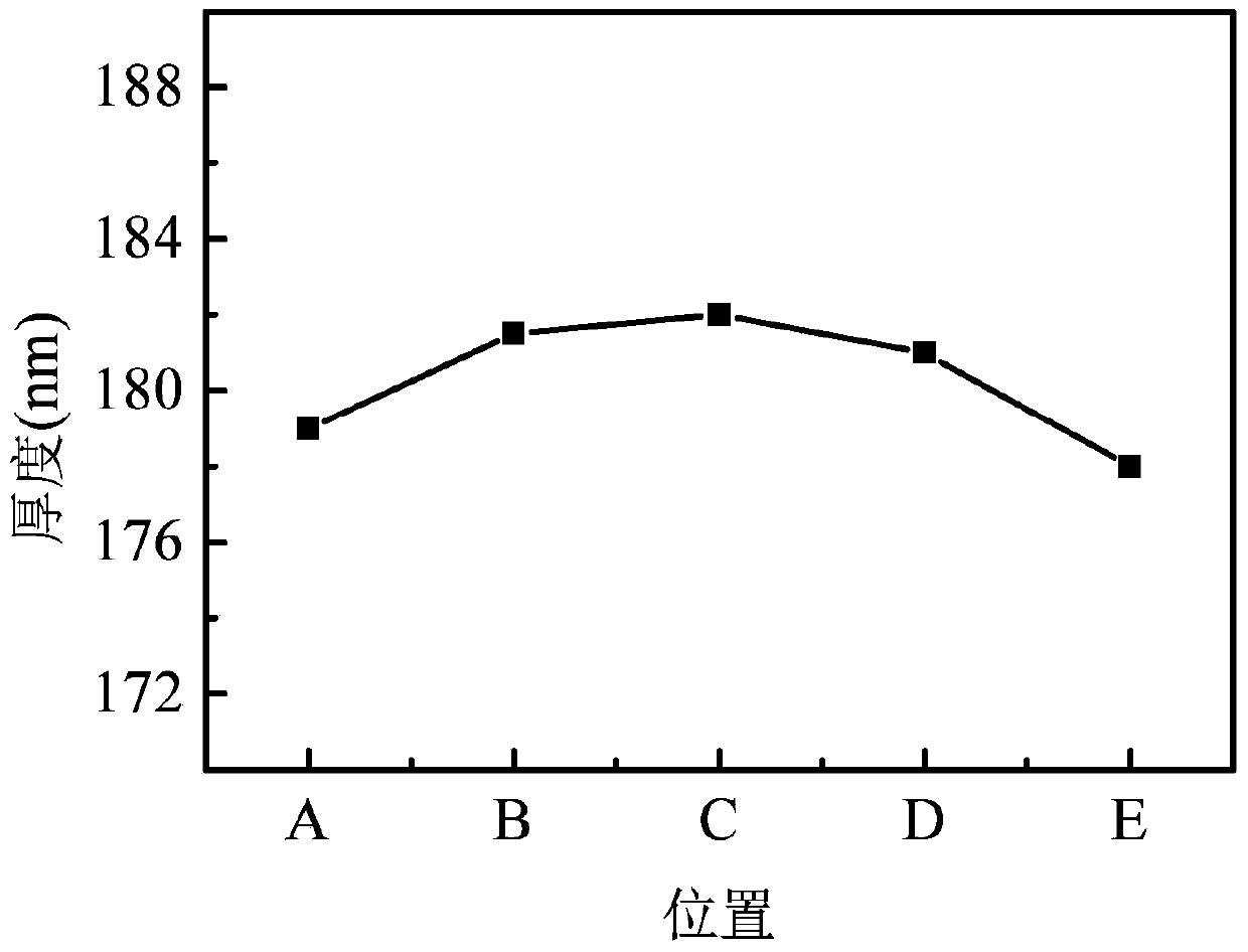
[0031] Combine Figure 1-3 . A GaN film grown on a sapphire substrate (see attached figure 1 ), including growing in Al 2 O 3 The substrate (11) and its (0001) plane are offset from the (10-10) plane by 0.2° (the crystal epitaxial orientation relationship is: the (0001) plane of GaN is parallel to Al 2 O 3 (0001) plane) as the AlN nucleation layer (12) on the crystal epitaxial growth, and the GaN film (13) grown on the AlN nucleation layer (12). The thickness of the AlN nucleation layer (12) is 8 nm, the thickness of the GaN thin film (13) is 180 nm, and the unevenness is 2.20%.

[0032] The method for preparing a GaN film grown on a sapphire substrate of this embodiment is prepared by the following steps:

[0033] a. Al 2 O 3 The substrate is cleaned and annealed; the specific annealing process is: put the substrate into an annealing chamber, and treat Al in a nitrogen atmosphere at 850°C. 2 O 3 The substrate is annealed for 1 hour; the cleaning is specifically: Al 2 O 3 The subs...

Embodiment 2

[0044] This embodiment is performed on the basis of embodiment 1, and the difference is that: the thickness of the AlN nucleation layer (12) is 10 nm, the thickness of the GaN film (13) is 100 nm, and the unevenness is 2.94 %.

Embodiment 3

[0046] This embodiment is carried out on the basis of embodiment 1, and the difference is that the thickness of the AlN nucleation layer (12) is 5nm, the thickness of the GaN thin film (13) is 200nm, and the unevenness is 2.47 %.


PUM

PropertyMeasurementUnit
Thicknessaaaaaaaaaa
Thicknessaaaaaaaaaa
Thicknessaaaaaaaaaa

Abstract

The invention relates to a high-uniformity GaN film growing on a sapphire substrate. The high-uniformity GaN film growing on the sapphire substrate comprises an Al2O3 substrate, an AlN nucleation layer and a GaN film body, wherein the AlN nucleation layer and the GaN film body sequentially grow in an epitaxial mode from the face (0001) of the Al2O3 substrate to the direction deviating from the face (10-10) by 0.2 degree. The invention further relates to a preparing method of the GaN film. The method includes the following steps that a, the Al2O3 substrate is cleaned and annealed; b, the AlN nucleation layer grows on the Al2O3 substrate treated through the step a in an epitaxial mode; c, the GaN film body grows on the AlN nucleation layer growing through the step b in an epitaxial mode. The high-uniformity GaN film growing on the sapphire substrate is used for preparing an LED, a photoelectric detector and a solar cell. The GaN film is low in cost, high in quality, high in uniformity and wide in application range.

Description

Technical field [0001] The invention relates to a GaN film and a preparation method and application thereof, in particular to a GaN film with high uniformity grown on a sapphire substrate, and a preparation method and application thereof. Background technique [0002] Compared with traditional light sources, light-emitting diodes (LEDs) have outstanding characteristics such as low power consumption, long life, high brightness, small size, strong adaptability and controllability, etc., and they are a new type of solid-state lighting source and green light source. It has a wide range of applications in the fields of exterior lighting and decoration engineering. Against the background of increasingly depleted petrochemical energy sources and increasingly severe global warming issues, energy conservation and emission reduction have become an important issue facing the world. A low-carbon economy based on low energy consumption, low pollution and low emissions will become an importan...

Claims


Application Information

Patent Timeline
IPC IPC(8): H01L21/205H01L33/00H01L33/02H01L31/18H01L31/0248
CPCH01L21/0242H01L21/02458H01L21/0254H01L21/0262Y02P70/50
Inventor 李国强
Owner HEYUAN CHOICORE PHOTOELECTRIC TECH CO LTD
Why Eureka
Try Eureka