Micro-polarizer array based on metal nano-grating and its preparation method
一种微偏振片阵列、金属纳米的技术,应用在偏振元件、光机械设备、图纹面的照相制版工艺等方向,能够解决增加制作成本、透射率低、降低所需光线透过率等问题,达到降低制作成本、简化工艺流程的效果
- Summary
- Abstract
- Description
- Claims
- Application Information
AI Technical Summary
Problems solved by technology
Method used
Image
Examples
preparation example Construction
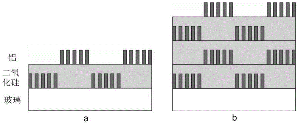
[0028] According to another aspect of the present invention, a method for preparing a single-layer micro-polarizer array based on a metal nanograting is provided, such as Figure 4 As shown, the preparation method includes the following steps:
[0029] Step 1. Perform double-sided polishing and cleaning on the substrate with high light transmittance. The substrate material is generally selected from materials with good transmission performance for light in the working band, such as glass or sapphire, and then electron beam deposition, chemical vapor deposition and chemical vapor deposition are used respectively. The spin coating method sequentially deposits an aluminum layer, a silicon dioxide layer and a negative photoresist layer on the base material. Among them, silicon dioxide is used as a hard template to etch the metal layer, such as Figure 4 shown in a;
[0030] Step 2. Use a laser to generate two beams of light to interfere, and the generated interference fringes expose t...
Embodiment 1
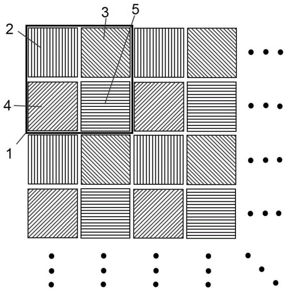
[0037] In the first embodiment, a micro-polarizer array with four polarization transmission directions is prepared according to the above method. The specific process is as follows:
[0038] Step 1. Use the glass substrate as the base material, optimize the glass surface through the mechanical chemical polishing (CMP) process, so that the fluctuation of the glass surface in the 3cm×3cm area is + / -5nm, and the glass sample is sequentially immersed in isopropanol and acetone Cleaning, the sample is then placed in a reactive ion etching device, and further cleaned with oxygen by reactive ion etching, wherein the etching power is 300W and the time is 20 minutes;
[0039] Step 2. Electron beam deposition and chemical vapor deposition are respectively used to plate 140nm aluminum and 20nm silicon dioxide on the surface of the sample. The silicon dioxide is used as a hard template to etch the aluminum layer;
[0040] Step 3. Spin-coat the negative photoresist onto the sample. The negative ...
PUM
 Abstract
Description
Claims
Application Information
 - R&D
- Intellectual Property
- Life Sciences
- Materials
- Tech Scout
- Unparalleled Data Quality
- Higher Quality Content
- 60% Fewer Hallucinations
Browse by: Latest US Patents, China's latest patents, Technical Efficacy Thesaurus, Application Domain, Technology Topic, Popular Technical Reports.
© 2025 PatSnap. All rights reserved.Legal|Privacy policy|Modern Slavery Act Transparency Statement|Sitemap|About US| Contact US: help@patsnap.com


