High-sensitivity cmos image sensor shared pixel structure
An image sensor and high-sensitivity technology, which is applied in the field of image sensors, can solve the problems of low photosensitive sensitivity of pixels and reduce photoelectric conversion gain, etc., and achieve the effect of improving photosensitive sensitivity and photoelectric conversion gain
- Summary
- Abstract
- Description
- Claims
- Application Information
AI Technical Summary
Problems solved by technology
Method used
Image
Examples
specific Embodiment approach
[0019] High-sensitivity CMOS image sensor sharing type pixel structure of the present invention, its preferred embodiment is:
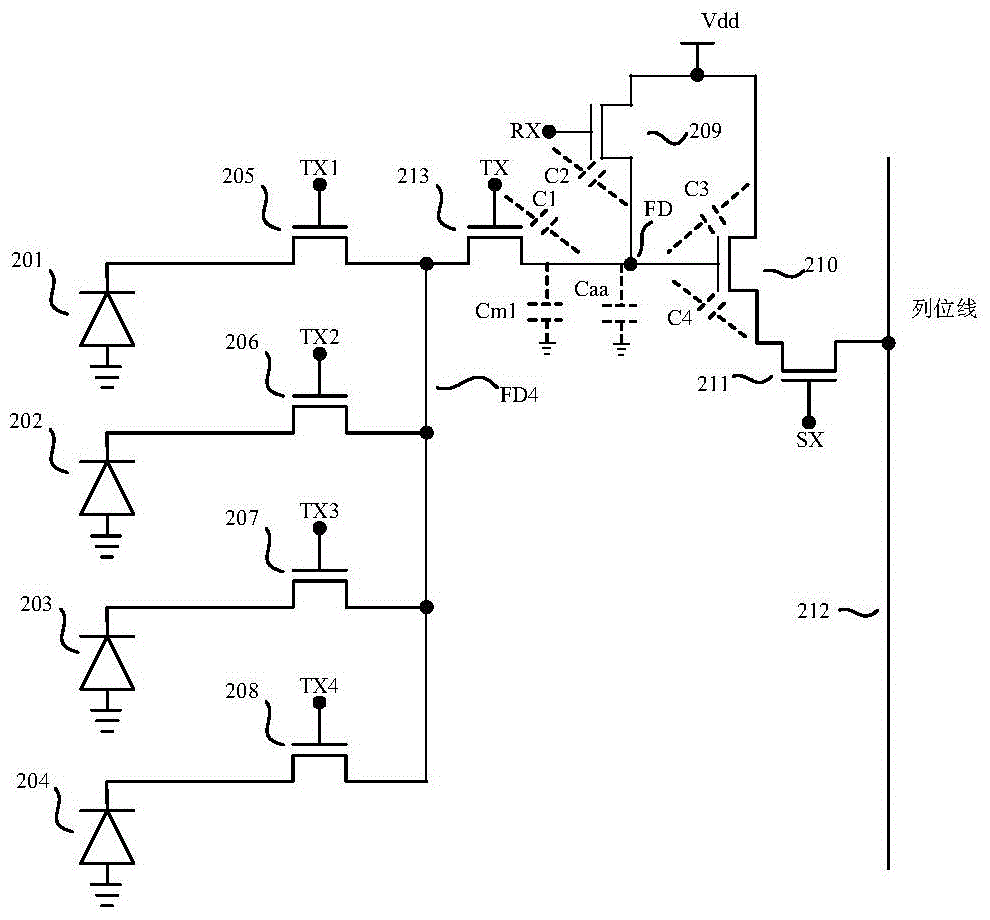
[0020] Including a plurality of photodiodes and the same number of charge transfer transistors and a first floating active area, and also includes a reset transistor, a source follower transistor, a row selection transistor and a second floating active area, the first floating active area The region is separated from the second floating active region by a switch transistor.
[0021] The drain of the switch transistor is connected to the second floating active region, and the source is connected to the first floating active region.
[0022] The gate of the source follower transistor is connected to the second floating active area, and the source follower transistor is used to detect the potential signal change of the second floating active area.
[0023] In the shared pixel structure of the high-sensitivity CMOS image sensor, the number of pixels incl...
specific Embodiment
[0030] In the embodiment of the present invention, the four-pixel sharing structure of a CMOS image sensor is taken as an example. In this pixel structure, Pin-type N-type photodiodes are used, and transistors in the pixels are N-type transistors.
[0031] Such as figure 2 As shown, it includes photodiodes 201-204 of four pixels in a shared structure, charge transfer transistors 205-208 in four pixels, reset transistor 209, source follower transistor 210, row selection transistor 211, column bit line 212, switching transistor 213; the gate terminals of the charge transfer transistors 205-208 are respectively TX1, TX2, TX3 and TX4, the gate terminals of the reset transistor 209 and the row selection transistor 211 are RX and SX, the gate terminals of the switch transistor 213 are TX, and Vdd is the power supply voltage ; FD4 is the first floating active area, FD is the second floating active area, C1 is the overlapping capacitance of FD and TX, C2 is the overlapping capacitanc...
PUM
 Abstract
Description
Claims
Application Information
 - R&D
- Intellectual Property
- Life Sciences
- Materials
- Tech Scout
- Unparalleled Data Quality
- Higher Quality Content
- 60% Fewer Hallucinations
Browse by: Latest US Patents, China's latest patents, Technical Efficacy Thesaurus, Application Domain, Technology Topic, Popular Technical Reports.
© 2025 PatSnap. All rights reserved.Legal|Privacy policy|Modern Slavery Act Transparency Statement|Sitemap|About US| Contact US: help@patsnap.com


