Semiconductor package and fabrication method thereof

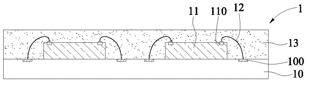
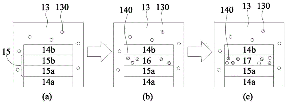
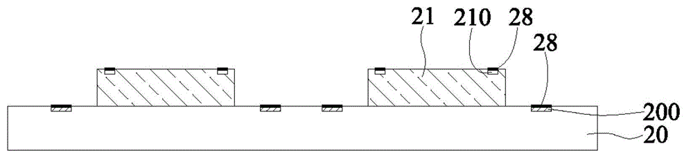
A technology for semiconductors and packages, applied in the field of semiconductor packages that can improve reliability and its manufacturing method, can solve the problems of increased corrosion rate, peeling of copper wires, easy corrosion of aluminum oxide layer 17, etc., and achieve corrosion rate Slow down, avoid electrical disconnection, improve the effect of corrosion resistance

Inactive Publication Date: 2014-07-09
SILICONWARE PRECISION IND CO LTD
View PDF7 Cites 0 Cited by
  • Summary
  • Abstract
  • Description
  • Claims
  • Application Information

AI Technical Summary

Problems solved by technology

[0011] However, alumina (Al 2 o 3 ) is an insulating substance with poor corrosion resistance, that is, the aluminum oxide layer 17 is easy to corrode, causing the corrosion rate of the aluminum oxide layer 17 to increase, thus causing the copper wire (that is, the copper material 14b or the wire 12 ) peeling, resulting in electrical disconnection of the semiconductor package 1, so that the reliability of the product is not good

Method used


Image

  • Semiconductor package and fabrication method thereof
  • Semiconductor package and fabrication method thereof
  • Semiconductor package and fabrication method thereof

Examples


Embodiment Construction

[0052] The following describes the implementation of the present invention through specific specific examples. Those skilled in the art can easily understand other advantages and effects of the present invention from the content disclosed in this specification.

[0053] It should be noted that the structure, ratio, size, etc. shown in the accompanying drawings in this specification are only used to match the content disclosed in the specification for the understanding and reading of those skilled in the art, and are not intended to limit the implementation of the present invention. Limited conditions, so it does not have technical significance. Any structural modification, proportional relationship change, or size adjustment should still fall under the present invention without affecting the effects and objectives that can be achieved by the present invention. The disclosed technical content must be within the scope of coverage. At the same time, terms such as "上" and "一" cited i...


PUM


Abstract

The invention relates to a semiconductor package and the fabrication method thereof. The semiconductor package includes a carrier having electrical connecting pads, a semiconductor element disposed on the carrier and having electrode pads, conductive elements electrically connected to the electrode pads and the electrical connecting pads, fluorine ions formed between the conductive elements and the electrode pads or between the conductive elements and the electrical connecting pads, and an encapsulant formed on the carrier and the conductive elements, wherein the electrode pads or the electrical connecting pads are formed by aluminum materials to form fluorine aluminum by way of packaging the fluorine ions after the completion of the packaging process. Accordingly, the corrosion resistance of the semiconductor package is increased.

Description

Technical field [0001] The invention relates to a semiconductor package and a manufacturing method thereof, in particular to a semiconductor package and a manufacturing method thereof that can improve reliability. Background technique [0002] With the vigorous development of the electronics industry, electronic products are gradually moving towards the trend of multi-function and high performance. Such as Figure 1A As shown, it discloses an existing wire-bonding type semiconductor package 1 in which a semiconductor chip 11 with a plurality of electrode pads 110 is arranged on a carrier 10 such as a lead frame or a package substrate, and then a wire 12 is used for electrical The electrical connection pad 100 (or the lead of the lead frame) that connects the semiconductor chip 11 and the carrier 10, and then wraps the semiconductor chip 11 and the wires 12 with an epoxy resin encapsulant 13 to pass the encapsulant 13 Protect the semiconductor chip 11 and the carrier 10, and preve...

Claims


Application Information

Patent Timeline
Patent Type & Authority Applications(China)
IPC IPC(8): H01L23/488H01L23/31H01L21/60
CPCH01L2924/365H01L2224/16501H01L23/293H01L23/3121H01L23/564H01L24/05H01L24/13H01L24/16H01L24/45H01L24/48H01L24/81H01L24/85H01L2224/0401H01L2224/04042H01L2224/05624H01L2224/13147H01L2224/16227H01L2224/16245H01L2224/45147H01L2224/48227H01L2224/48245H01L2224/48465H01L2224/48507H01L2224/48824H01L2224/81191H01L2224/81424H01L2224/8181H01L2224/85424H01L2224/8581H01L2224/97H01L2924/00015H01L2224/48505H01L2224/16503H01L2224/4852H01L2224/48463H01L2224/45015H01L2224/45144H01L2224/48247H01L2224/48624H01L2224/16225H01L2924/181H01L24/97H01L2924/00014H01L2924/00012H01L2924/0583H01L2924/01013H01L2224/85H01L2224/81H01L2924/00
Inventor 洪隆棠林伟胜叶孟宏
Owner SILICONWARE PRECISION IND CO LTD
Why Eureka
Try Eureka