Quantum dot luminescent device
A quantum dot luminescence and quantum dot technology, applied in the field of quantum dots, can solve the problems of low luminous efficiency, achieve the effects of ensuring electrical neutrality, improving working life, and improving external quantum efficiency
- Summary
- Abstract
- Description
- Claims
- Application Information
AI Technical Summary
Problems solved by technology
Method used
Image

Examples
Embodiment 1
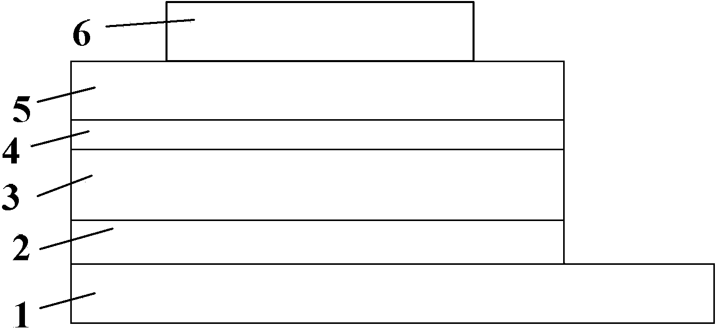
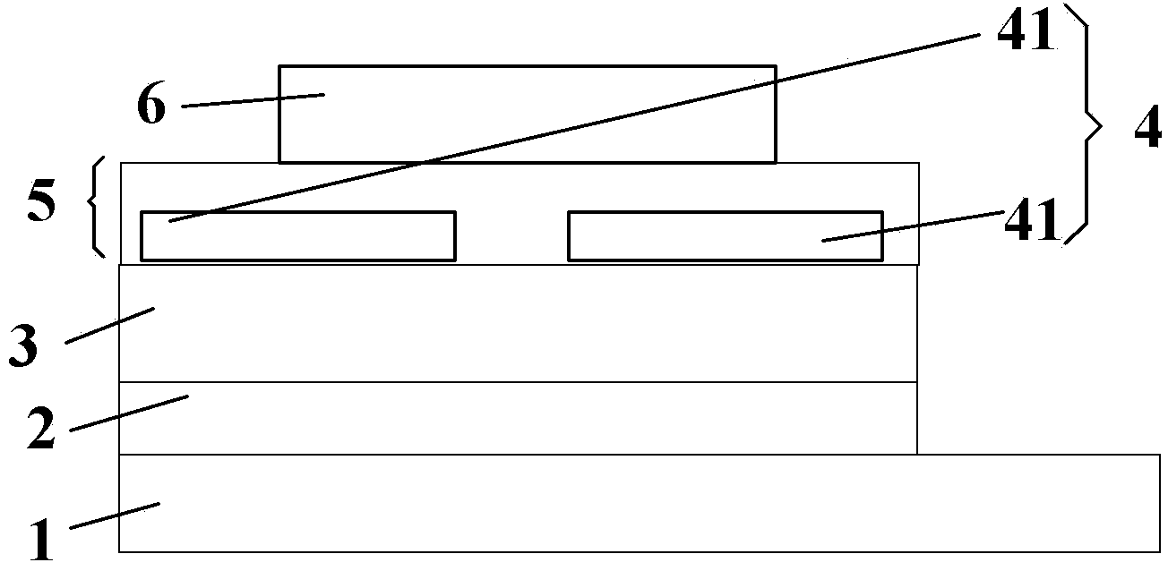
[0068] 1) Cleaning of glass substrates containing ITO transparent electrodes (i.e., anodes): cleaning with deionized water and ethanol and continuous ultrasonic treatment for 15 minutes, then quickly drying the liquid with a nitrogen gun, and treating it under oxygen plasma for 10 minutes, To clean the ITO surface and improve the work function of the ITO electrode;
[0069] 2) Fabrication of the hole transport layer: in air, spin-coat PEDOT:PSS on the cleaned glass substrate at a speed of 4000 rpm, and the spin-coating time is 1 minute. Anneal 20min, dry the liquid that has not evaporated, then transfer into the glove box (O 2 2 O<5ppm), annealed again at 130°C for 10min to form a PEDOT:PSS layer; then spin-coat poly-TPD chlorobenzene solution (concentration 8mg / ml) on the PEDOT:PSS layer at a speed of 2000 rpm, spin coating time 45s. After the spin coating is completed, anneal at 110°C for 30 minutes in a glove box to form a poly-TPD layer; then spin coat a PVK m-xylene solu...
Embodiment 2
[0075] 1), cleaning of glass substrates containing ITO transparent electrodes: same as in Example 1;
[0076] 2) Fabrication of the hole transport layer: in air, spin-coat PEDOT:PSS on the cleaned glass substrate at a speed of 4000 rpm, and the spin-coating time is 1 minute. Anneal 20min, dry the liquid that has not evaporated, then transfer into the glove box (O 2 2 O<5ppm), annealed again at 130°C for 10min to form a PEDOT:PSS layer; then spin-coated a poly-TPD chlorobenzene solution (concentration of 8mg / ml) on the PEDOT:SS layer at a speed of 2000 rpm, spin-coating time 45s, after the spin coating is completed, anneal at 110°C for 30 minutes in a glove box to form a poly-TPD layer;
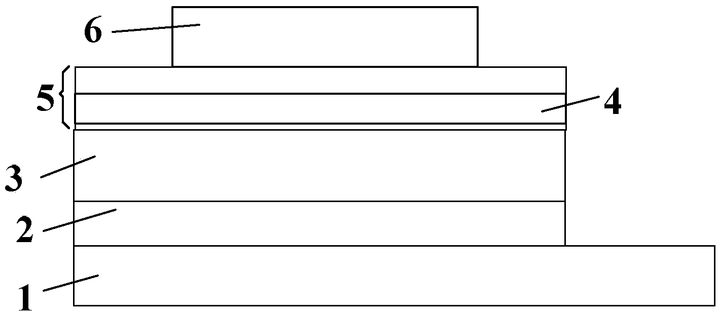
[0077] 3), the production of quantum dot light-emitting layer: the same as Example 1;
[0078] 4) Fabrication of the electron blocking layer: same as in Example 1;
[0079] 5), the production of electron transport layer: same as embodiment 1;
[0080] 6), cathode: same as embodiment 1.
Embodiment 3
[0082] 1), cleaning of glass substrates containing ITO transparent electrodes: same as in Example 1;
[0083] 2) Fabrication of the hole transport layer: in air, spin-coat PEDOT:PSS on the cleaned glass substrate at a speed of 4000 rpm, and the spin-coating time is 1 minute. Anneal 20min, dry the liquid that has not evaporated, then transfer into the glove box (O 2 2 O<5ppm), then annealed at 130°C for 10min to form a PEDOT:PSS layer;
[0084] 3), the production of quantum dot light-emitting layer: the same as Example 1;
[0085] 4) Fabrication of the electron blocking layer: same as in Example 1;
[0086] 5), the production of electron transport layer: same as embodiment 1;
[0087] 6), cathode: same as embodiment 1.
PUM
| Property | Measurement | Unit |
|---|---|---|
| Thickness | aaaaa | aaaaa |
| Thickness | aaaaa | aaaaa |
| Thickness | aaaaa | aaaaa |
Abstract
Description
Claims
Application Information
 - R&D
- Intellectual Property
- Life Sciences
- Materials
- Tech Scout
- Unparalleled Data Quality
- Higher Quality Content
- 60% Fewer Hallucinations
Browse by: Latest US Patents, China's latest patents, Technical Efficacy Thesaurus, Application Domain, Technology Topic, Popular Technical Reports.
© 2025 PatSnap. All rights reserved.Legal|Privacy policy|Modern Slavery Act Transparency Statement|Sitemap|About US| Contact US: help@patsnap.com