DC/DC converter and display device including the same
A DC converter, a significant technology, applied in the direction of output power conversion devices, instruments, control/regulation systems, etc., can solve the problems that EMI cannot be reduced, oscillation components cannot be fundamentally eliminated, etc., and the number of components can be reduced and reduced The effect of EMI
- Summary
- Abstract
- Description
- Claims
- Application Information
AI Technical Summary
Problems solved by technology
Method used
Image
Examples
no. 1 approach
[0070] In a display device, in order to generate power for various ICs such as a driver IC and a timing controller for driving a display device, a power supply circuit (DC / DC converter) that receives a single input voltage and generates power for various ICs is used . A block diagram of the entire display device is shown in Figure 13 middle.
[0071] Generally, in the case of a step-up circuit or a step-down circuit, a DC / DC converter is constituted by components or elements such as an inductor 4 , a rectification diode 6 , a field effect transistor (FET), and a smoothing capacitor (C).
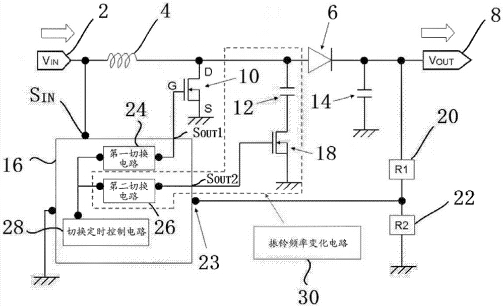
[0072] will use equal to V IN the input voltage and is equal to V OUT The output voltage description of the figure 1 The DC / DC converter circuit (boost circuit) shown.
[0073] exist figure 1 Among them, the DC / DC converter of the present invention has a signal input terminal V IN 2 series connected inductor 4, rectifier diode 6, and V IN 2 is connected to the input S of the DC / DC ...
no. 2 approach
[0153] In the first embodiment, an example in which the first switching circuit 24 and the second switching circuit 26 are controlled and the ringing frequency varying circuit 30 is driven using the switching timing control circuit 28 has been described. In the second embodiment, an example of a configuration using a simple delay circuit without using the switching timing control circuit 28 will be described.
[0154] Figure 8 is the circuit configuration diagram. Through this action, such as Figure 9 As shown, a waveform delayed by using the timing of the switching circuit is formed.
[0155] will mainly be paired with figure 1 The differences are explained. Figure 8 neutralize figure 1 The biggest difference of the first embodiment shown is the DC / DC oscillation circuit IC (for booster) 34 . In the DC / DC oscillation circuit IC (for boosting voltage) 34 , a delay control circuit 32 is provided instead of the second switching circuit 26 . The delay control circuit ...
PUM
 Abstract
Description
Claims
Application Information
 - R&D Engineer
- R&D Manager
- IP Professional
- Industry Leading Data Capabilities
- Powerful AI technology
- Patent DNA Extraction
Browse by: Latest US Patents, China's latest patents, Technical Efficacy Thesaurus, Application Domain, Technology Topic, Popular Technical Reports.
© 2024 PatSnap. All rights reserved.Legal|Privacy policy|Modern Slavery Act Transparency Statement|Sitemap|About US| Contact US: help@patsnap.com


