Method for manufacturing MOS grid device

A manufacturing method and gate technology, which are used in semiconductor/solid-state device manufacturing, semiconductor devices, electrical components, etc., can solve the problems of increasing manufacturing difficulty and cost, inability to achieve current density, and many steps, and reduce etching. Process difficulty, ensuring uniformity and consistency, and reducing the effect of area

Inactive Publication Date: 2014-06-11
宁波达新半导体有限公司 +1
View PDF8 Cites 2 Cited by
  • Summary
  • Abstract
  • Description
  • Claims
  • Application Information

AI Technical Summary

Problems solved by technology

[0012] It can be seen from the above that in the existing method, the alignment requirements of the lithography process in the opening area are relatively high, and the alignment requirements of the lithography process in the source area are also relatively high, which will result in a large number of steps requiring high lithography alignment. , which increases manufacturing difficulty and cost, and provides a possible source of device defects, and due to the limitation of mask process capability, the current density cannot be made larger

Method used


Image

  • Method for manufacturing MOS grid device
  • Method for manufacturing MOS grid device

Examples


Embodiment Construction

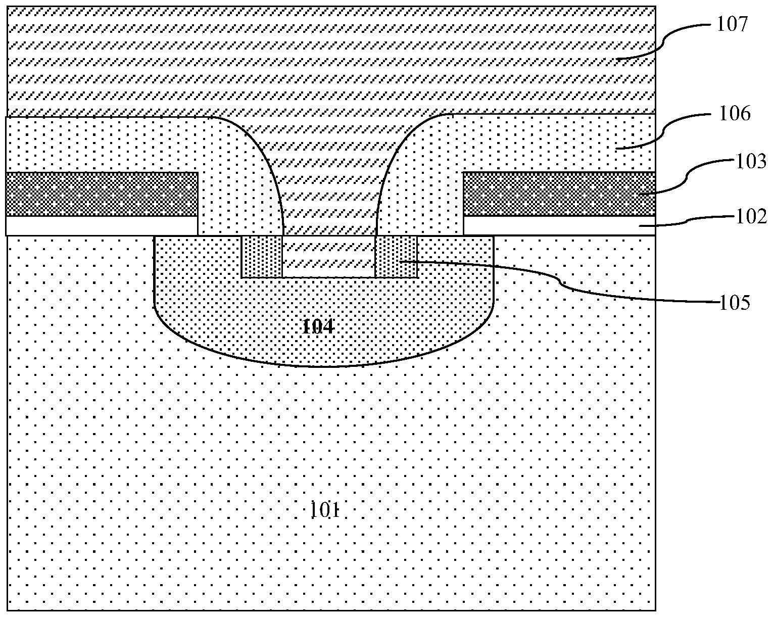
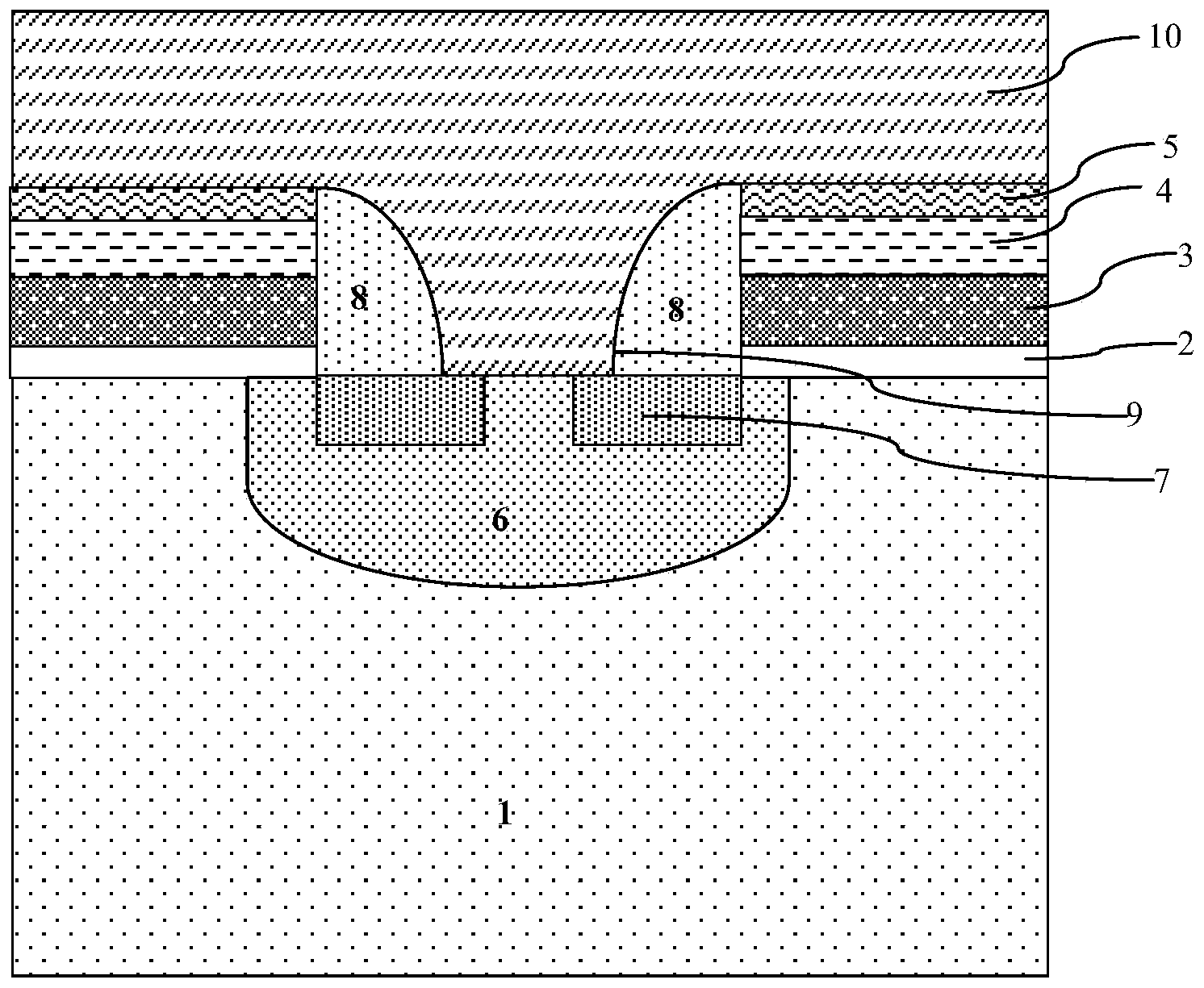
[0032] Such as figure 2 Shown is a structural diagram of the MOS gate device formed by the method of the embodiment of the present invention. The MOS gate device in the embodiment of the present invention includes a power MOSFET, a MOS gate thyristor, an insulated gate bipolar transistor, and a gate turn-off device. The manufacturing method of the MOS gate device in the embodiment of the present invention includes steps:

[0033] Step 1: Provide a semiconductor substrate 1 , and sequentially form a gate dielectric layer 2 , a gate layer 3 , a gate booster layer 4 and an etch stop layer 5 on the surface of the semiconductor substrate 1 . Preferably, the semiconductor substrate 1 is a silicon substrate, the gate dielectric layer 2 is an oxide layer, the gate layer 3 is a polysilicon layer, and the gate booster layer 4 is an oxide layer.

[0034] Step 2, using a photolithographic etching process to form a gate pattern structure, the gate is composed of the etched gate dielectri...


PUM


Abstract

The invention discloses a method for manufacturing an MOS grid device. The method includes the following steps that a grid medium layer, a grid layer, a grid heightening layer and an etching retaining layer are sequentially formed on the surface of a semiconductor substrate; the photoetching technology is used for forming a grid graph structure; a body zone is formed; a source zone is formed by photoetching through the filling technology; a side wall layer is deposited; comprehensive etching is carried out on the side wall layer and a relative-width side wall is formed; the etching technology is adopted and autoregistration etching is carried out on the relative-width side wall to form a grid hole forming zone and a source zone hole forming zone; a front face metal layer is deposited; a front face electrode leading-out terminal is formed through photoetching in an etching mode. Compared with a traditional photomask registration technology, the requirement for photoetching precision is lowered. Meanwhile, the evenness and uniformity of the relative-width side wall are ensured, and therefore defects caused by the mask technology and the limitation on the current density are reduced, device density can be improved, and therefore the integration degree is improved. In addition, the additional etching barrier layer can also lower the precision requirement for the etching technology and the difficulty of the etching technology is lowered.

Description

technical field [0001] The invention relates to a manufacturing process method of a semiconductor integrated circuit, in particular to a manufacturing method of a MOS gate device. Background technique [0002] MOS gate devices are well known in the art, and these devices include power MOSFETS, MOS gate thyristors, insulated gate bipolar transistors (IGBTs), gate turn-off devices, and the like. [0003] Existing fabrication methods for MOS gate devices typically include many plate-making masking steps with strict mask alignment steps, each of which increases manufacturing time and cost and provides a possible source of device defects , and due to the limitation of the mask process capability, the current density cannot be made larger. Such as figure 1 Shown is a structure diagram of a MOS gate device formed by an existing method. The manufacturing method of the existing MOS gate device comprises the following steps: [0004] Step 1: Provide a semiconductor substrate such ...

Claims


Application Information

Patent Timeline
Patent Type & Authority Applications(China)
IPC IPC(8): H01L21/336H01L21/331
CPCH01L29/66477
Inventor 陈智勇孙娜
Owner 宁波达新半导体有限公司
Why Eureka
Try Eureka