Method for manufacturing a nitride semiconductor light emitting device and nitride semiconductor light emitting device manufactured thereby

A technology for nitride semiconductors and light-emitting devices, which is applied to semiconductor devices, electrical components, circuits, etc., can solve the problems of increasing the area of ​​the barrier metal layer and reducing the light-emitting area, and achieves the reduction of the area, the increase of the light-emitting area, and the simplification of the light-emitting area. The effect of the manufacturing process

Inactive Publication Date: 2014-05-14
SAMSUNG ELECTRONICS CO LTD
View PDF5 Cites 6 Cited by
  • Summary
  • Abstract
  • Description
  • Claims
  • Application Information

AI Technical Summary

Problems solved by technology

Here, when the distance between the barrier metal layer and the electrode is increased, the area of ​​the barrier metal layer increases, resulting in a decrease in the light emitting area.

Method used


Image

  • Method for manufacturing a nitride semiconductor light emitting device and nitride semiconductor light emitting device manufactured thereby
  • Method for manufacturing a nitride semiconductor light emitting device and nitride semiconductor light emitting device manufactured thereby
  • Method for manufacturing a nitride semiconductor light emitting device and nitride semiconductor light emitting device manufactured thereby

Examples


Embodiment Construction

[0030] Exemplary embodiments of the present invention will now be described in detail with reference to the accompanying drawings.

[0031] This invention may, however, be embodied in many different forms and should not be construed as limited to the specific embodiments set forth herein. Rather, these embodiments are provided so that this disclosure will be thorough and complete, and will fully convey the scope of the invention to those skilled in the art. In the drawings, the shapes and dimensions of elements may be exaggerated for clarity, and the same reference numerals will be used throughout to designate the same or like elements.

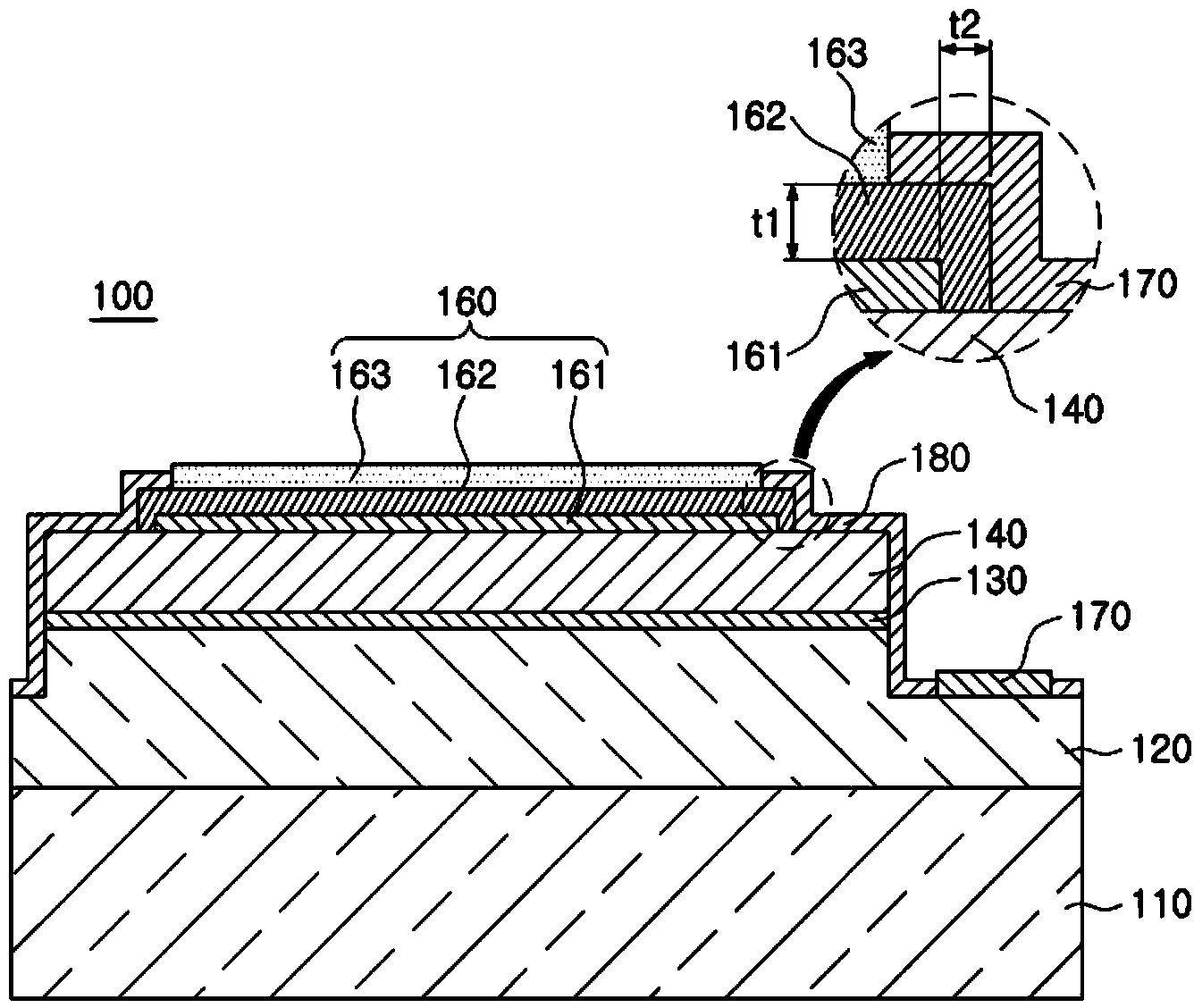
[0032] figure 1 is a cross-sectional side view schematically showing a nitride semiconductor light emitting device according to an exemplary embodiment of the present invention.

[0033] refer to figure 1 , the nitride semiconductor light emitting device 100 according to an exemplary embodiment of the present invention may include a first ...


PUM


Abstract

According to one aspect of the present invention, provided are a method for manufacturing a nitride semiconductor light emitting device and a nitride semiconductor light emitting device manufactured thereby. The method for manufacturing the nitride semiconductor light emitting device comprises the steps of: forming first and second conductive-type nitride semiconductor layers on a substrate to form a light emitting structure including an active layer between the first and second conductive-type nitride semiconductor layers; successively forming the first conductive-type nitride semiconductor layer, the active layer, and the second conductive-type nitride semiconductor layer; forming a first electrode connected to the first conductive-type nitride semiconductor layer; forming a photoresist film on the second conductive-type nitride semiconductor layer to expose a portion of the second conductive-type nitride semiconductor layer; and removing the photoresist film after a reflective metal layer serving as a second electrode and a barrier layer are successively formed on the second conductive-type nitride semiconductor layer exposed by the photoresist film.

Description

technical field [0001] The present invention relates to a method for manufacturing a nitride semiconductor light-emitting device and a nitride semiconductor light-emitting device manufactured by using the method, in particular to a method for manufacturing a nitride semiconductor light-emitting device, which can be achieved by simplifying the process for forming electrodes. To reduce the number of photoresist and photolithography steps while increasing the light emitting area of ​​the active layer. Background technique [0002] In recent years, with the development of light-emitting devices capable of emitting blue, green, and ultraviolet light using gallium nitride (GaN)-based compound semiconductors, it has become possible to display colors in a full color gamut. GaN-based compound semiconductor crystals can be grown on an insulating substrate such as a sapphire substrate, but for this reason, electrodes cannot be formed on the back surface of the substrate. Therefore, bo...

Claims


Application Information

Patent Timeline
Patent Type & Authority Applications(China)
IPC IPC(8): H01L33/36H01L33/46
CPCH01L33/405H01L33/44H01L2933/0016
Inventor 黄硕珉李进馥张泰盛禹锺均
Owner SAMSUNG ELECTRONICS CO LTD
Why Eureka
Try Eureka