Preparation method of thin film transistor, thin film transistor and display panel

A technology of thin film transistors and semiconductors, applied in the direction of transistors, semiconductor/solid-state device manufacturing, electric solid-state devices, etc., can solve the problems of low carrier mobility, disordered shape distribution, and small grain size in polysilicon, and achieve Effects of reducing grain boundary defects, simplifying the process, and improving stability

Inactive Publication Date: 2014-04-02
BEIJING BOE OPTOELECTRONCIS TECH CO LTD
View PDF4 Cites 7 Cited by
  • Summary
  • Abstract
  • Description
  • Claims
  • Application Information

AI Technical Summary

Problems solved by technology

[0004] Most of the polysilicon thin film transistors prepared by the above method are formed by inducing amorphous silicon by crystallization method. In the process of inducing amorphous silicon to form polysilicon, amorphous silicon spontaneously and slowly crystallizes along the direction of energy induction to form crystals. Grains, the grains formed in this spontaneous state, due to the low degree of crystallization, the size of the formed grains is small and the morphological distribution is out of order, so that when the grains are integrated to form polysilicon, the mobility of carriers in the polysilicon not tall

Method used


Image

  • Preparation method of thin film transistor, thin film transistor and display panel
  • Preparation method of thin film transistor, thin film transistor and display panel
  • Preparation method of thin film transistor, thin film transistor and display panel

Examples


Embodiment Construction

[0033] The following will clearly and completely describe the technical solutions in the embodiments of the present invention with reference to the accompanying drawings in the embodiments of the present invention. Obviously, the described embodiments are only some, not all, embodiments of the present invention. Based on the embodiments of the present invention, all other embodiments obtained by persons of ordinary skill in the art without making creative efforts belong to the protection scope of the present invention.

[0034] A method for manufacturing a thin film transistor, a thin film transistor, and a display panel provided by embodiments of the present invention will be described in detail below with reference to the accompanying drawings.

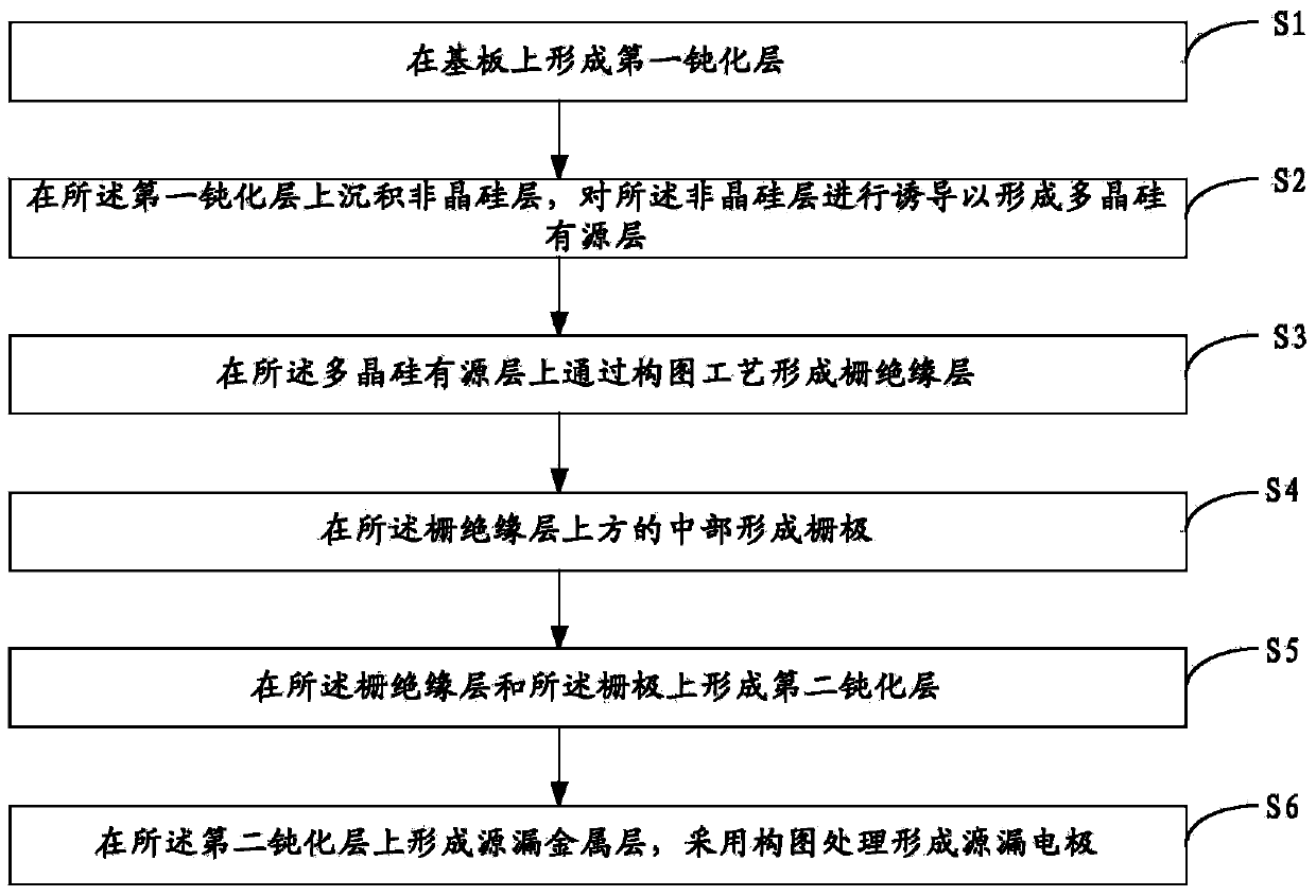
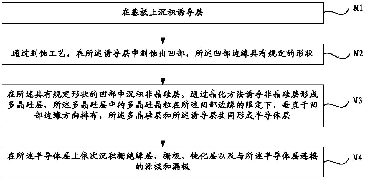
[0035] figure 2 It is a flow chart of the manufacturing method of the thin film transistor provided by the embodiment of the present invention. Such as figure 2 As shown, the preparation method provided by the embodiments of the...


PUM


Abstract

The embodiment of the invention provides a preparation method of a thin film transistor, the thin film transistor and a display panel, and belongs to the field of liquid crystal display, which aims at improving the mobility of carriers in polycrystalline silicone. The preparation method of the thin film transistor comprises the following steps of M1, depositing an induction layer on a substrate; M2, etching a concave part in the induction layer through the etching process, wherein the edge of the concave part is in a specifical shape; M3, depositing a non-crystalline silicone layer in the specifically-shaped concave part, inducing the non-crystalline silicone layer to form a polycrystalline silicone layer through a crystallizing method, arranging the polycrystalline silicone particles in the polycrystalline silicone in the direction vertical to the edge of the concave part by the limitation of the edge of the concave part, and enabling the polycrystalline silicone layer and the induction layer to form a semiconductor layer; M4, respectively depositing a grid insulation layer, a grid, a passivating layer, a source and a drain on the semiconductor layer, wherein the source and the drain are connected with the semiconductor layer. The method can be used for manufacturing the thin film transistor.

Description

technical field [0001] The invention relates to the field of liquid crystal display, in particular to a preparation method of a thin film transistor, a thin film transistor and a display panel. Background technique [0002] In recent years, with the continuous development of polysilicon TFT (Thin Film Transistor, thin film transistor) technology, its application has become more and more extensive, and it is regarded as an ideal substitute for amorphous silicon thin film transistor. Compared with amorphous silicon thin film transistors, polycrystalline silicon thin film transistors have the characteristics of high mobility, high integration and high resolution, and can provide brighter and more detailed images. [0003] In the prior art, thin film transistors are mostly prepared by the following methods, such as figure 1 As shown, step S1: forming a first passivation layer on the substrate; step S2: depositing an amorphous silicon layer on the first passivation layer, and in...

Claims


Application Information

Patent Timeline
Patent Type & Authority Applications(China)
IPC IPC(8): H01L29/06H01L29/786H01L21/336
CPCH01L21/02532H01L21/02658H01L21/02667H01L29/04H01L29/66757H01L29/78675H01L21/02672H01L27/1281H01L21/0217H01L21/02592H01L21/31111H01L29/78603
Inventor 李婧谢振宇陈旭张文余徐达
Owner BEIJING BOE OPTOELECTRONCIS TECH CO LTD
Why Eureka
Try Eureka