Limited random frequency difference reflection control method of microwave signal
A control method and microwave signal technology, applied in the direction of amplitude-to-angle modulation conversion, etc., can solve the problems of discontinuous frequency difference, limited cable length, limited simulation range, etc.
- Summary
- Abstract
- Description
- Claims
- Application Information
AI Technical Summary
Problems solved by technology
Method used
Image

Examples
Embodiment 1
[0027] In the present invention, the input signal is coupled out one way, and after wave detection, it is collected by DAC, and then after data processing, power detection is performed. If the power is large, a corresponding voltage is inserted through DAC, and attenuated by a voltage-controlled attenuator. , it remains unchanged, and finally adjusted to match the power range suitable for the modulator, which is used as the local oscillator signal input of the modulator. The required frequency difference digital signal is generated by FPGA or equivalent digital circuit. After digital-to-analog conversion by DAC, it is divided into sin signal and cos signal. After multiplication inside the modulator, a single sideband signal, carrier and The image frequency signal is suppressed to a certain extent. The signal output by the modulator is output after passing through a multi-stage power attenuator and amplitude stabilization loop after being adjusted to the power required by the u...
Embodiment 2
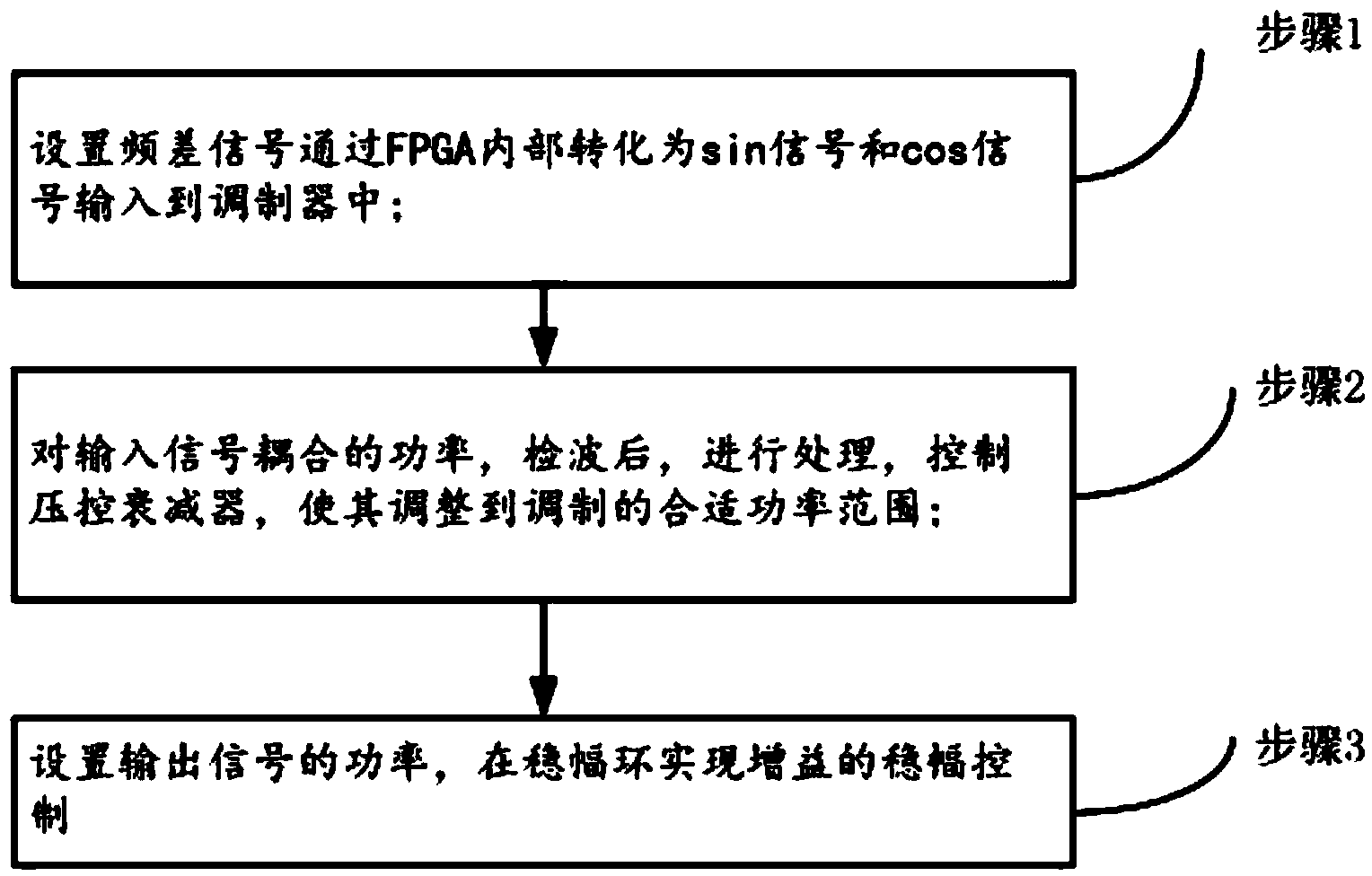
[0039] On the basis of above-mentioned embodiment, further as figure 1 As shown, a limited arbitrary frequency difference reflection control method for microwave signals is provided, which includes the following steps:
[0040] Step 1, set the frequency difference signal to be converted into a sin signal and a cos signal through the FPGA and input to the modulator;
[0041] Step 2, after detecting the coupled power of the input signal, process it, and control the voltage-controlled attenuator to adjust it to a suitable power range for modulation;
[0042] In step 3, the power of the output signal is set, and the amplitude stabilization control of the gain is realized in the amplitude stabilization loop.
[0043]Step A1 is also executed after the step 1: adjust the digital values of the modulator's amplitude, phase, and delay settings through the FPGA to calibrate.
[0044] In the step 1, the sin signal and the cos signal are multiplied inside the modulator to generate a si...
PUM
 Abstract
Description
Claims
Application Information
 - R&D
- Intellectual Property
- Life Sciences
- Materials
- Tech Scout
- Unparalleled Data Quality
- Higher Quality Content
- 60% Fewer Hallucinations
Browse by: Latest US Patents, China's latest patents, Technical Efficacy Thesaurus, Application Domain, Technology Topic, Popular Technical Reports.
© 2025 PatSnap. All rights reserved.Legal|Privacy policy|Modern Slavery Act Transparency Statement|Sitemap|About US| Contact US: help@patsnap.com