Defect detecting apparatus, defect correction device and defect detecting method
A defect detection and defect technology, applied in the direction of optical test defects/defects, optics, instruments, etc., can solve the problems of complex and expensive optical systems
- Summary
- Abstract
- Description
- Claims
- Application Information
AI Technical Summary
Problems solved by technology
Method used
Image

Examples
Embodiment Construction
[0037] Hereinafter, embodiments of the present invention will be described with reference to the drawings. In the following description, the same reference numerals are assigned to the same components. Their names and functions are also the same. Therefore, detailed descriptions about them are not repeated.
[0038] [device structure]
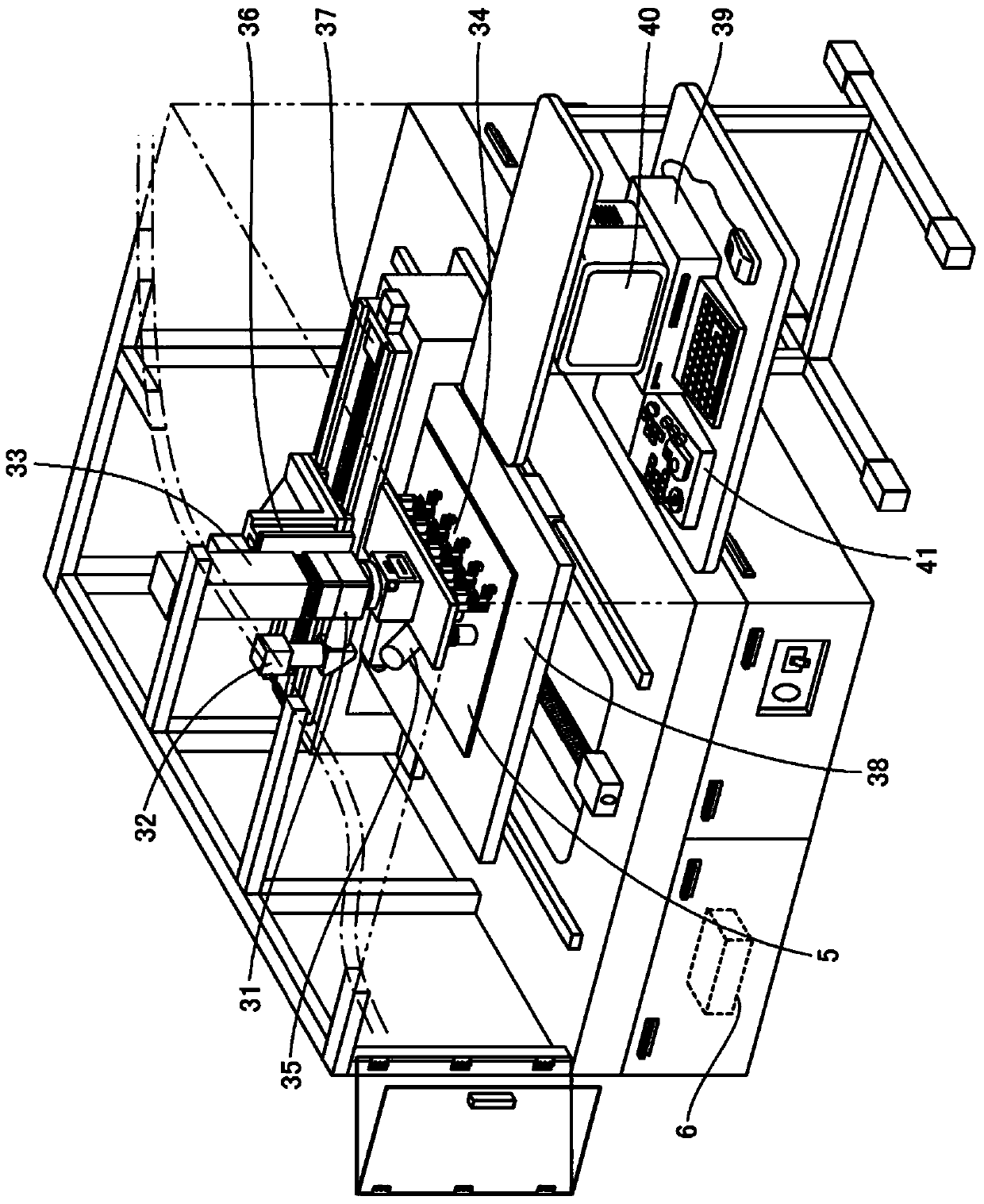
[0039] figure 1 It is a figure which shows the overall structure of the defect correction apparatus 100 in this embodiment. The defect correction device 100 includes: a correction head composed of an observation optical system 31, a CCD (Charge Coupled Device) camera 32, a laser device 33 for cutting, an ink coating mechanism 34, and a light source for ink curing. 35 constitutes; Z-axis worktable 36, and this Z-axis worktable 36 moves this correcting head in the direction (Z-axis direction) perpendicular to the liquid crystal color filter substrate 5 of correction object; X-axis worktable 37, this The X-axis table 37 mounts the Z-axis tabl...
PUM
 Abstract
Description
Claims
Application Information
 - R&D
- Intellectual Property
- Life Sciences
- Materials
- Tech Scout
- Unparalleled Data Quality
- Higher Quality Content
- 60% Fewer Hallucinations
Browse by: Latest US Patents, China's latest patents, Technical Efficacy Thesaurus, Application Domain, Technology Topic, Popular Technical Reports.
© 2025 PatSnap. All rights reserved.Legal|Privacy policy|Modern Slavery Act Transparency Statement|Sitemap|About US| Contact US: help@patsnap.com