Sensing circuit

A circuit and resistance technology, applied in the field of sensing circuits, can solve the problems of increasing the influence of process changes, increasing the difficulty of reading data accurately, and achieving the effect of enhancing the sensing margin

Active Publication Date: 2014-03-05
QUALCOMM INC
View PDF7 Cites 2 Cited by
  • Summary
  • Abstract
  • Description
  • Claims
  • Application Information

AI Technical Summary

Problems solved by technology

As memory devices get smaller, the influence of process variations increases, thereby increasing the difficulty of accurately reading data

Method used


Image

  • Sensing circuit
  • Sensing circuit
  • Sensing circuit

Examples


Embodiment Construction

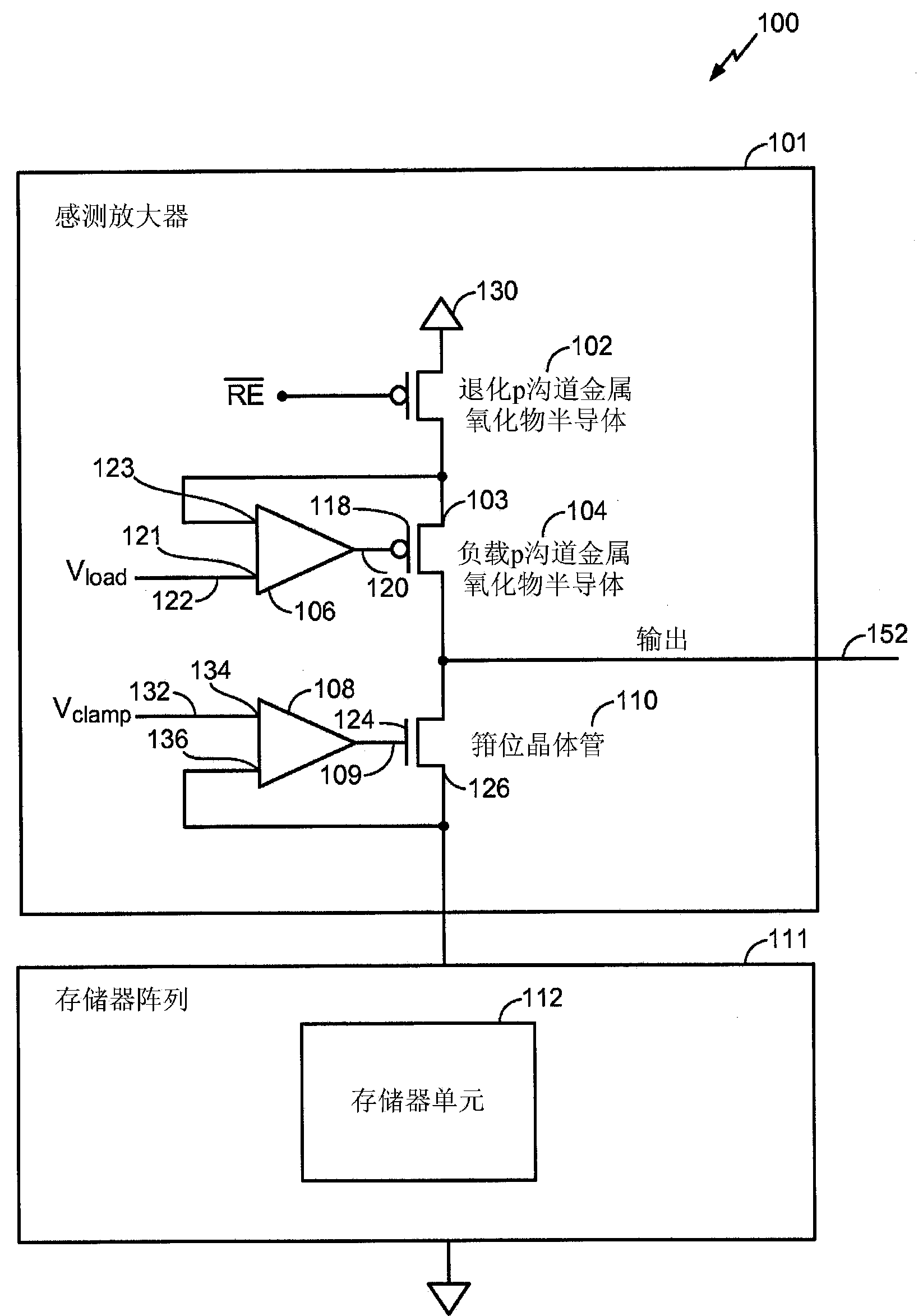
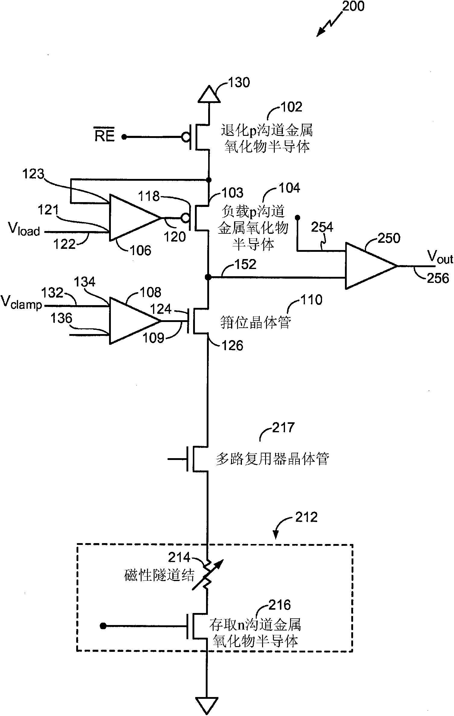
[0017] See figure 1 , A diagram of the first illustrative embodiment of the sensing circuit is disclosed, and it is generally indicated as 100. The sense circuit 100 includes a sense amplifier 101 coupled to the memory array 111. The memory array 111 includes a plurality of memory cells such as the illustrated memory cell 112. The memory array 111 generally includes a plurality of memory cells 112. The memory array 111 may be a magnetoresistive random access memory (MRAM), a phase change random access memory (PRAM), or a spin torque transfer MRAM (STT-MRAM), as an illustrative example.

[0018] The sense amplifier 101 includes a degraded PMOS transistor 102, a load PMOS transistor 104, and a clamp transistor 110. The sense amplifier 101 further includes a power supply 130, an output voltage 152, a first operational amplifier circuit 106 and a second operational amplifier circuit 108.

[0019] The clamp transistor 110 is configured to clamp the voltage applied to the resistance-b...


PUM


Abstract

A circuit (101) includes a degeneration p-channel metal - oxide - semiconductor (PMOS) transistor (102), a load PMOS transistor (104), and a clamp transistor (110) configured to clamp a voltage applied to a resistance based memory element (112) during a sensing operation. A gate of the load PMOS transistor (118) is controlled by an output (120) of an operational amplifier (106).

Description

Technical field [0001] The present invention generally relates to sensing circuits. Background technique [0002] Advances in technology have produced smaller and more powerful computing devices. For example, there are currently a variety of portable personal computing devices, including wireless computing devices, such as portable wireless phones, personal digital assistants (PDAs), and paging devices that are small, lightweight, and easy to carry by users. More specifically, portable wireless phones such as cellular phones and Internet Protocol (IP) phones can communicate voice and data packets via wireless networks. In addition, many such wireless telephones include other types of devices incorporated therein. For example, wireless phones may also include digital still cameras, digital video cameras, digital recorders, and audio file players. [0003] Advances in non-volatile memory technology include resistance-based memories, such as magnetic random access memory (MRAM). M...

Claims


Application Information

Patent Timeline
Patent Type & Authority Applications(China)
IPC IPC(8): G11C7/06G11C7/12G11C11/16G11C16/26G11C11/4091
CPCG11C11/1673G11C7/067G11C16/26G11C7/12G11C11/4091G11C13/004G11C11/1655G11C2207/002G11C7/06
Inventor 金圣克金吉苏刘景昊升·H·康
Owner QUALCOMM INC
Why Eureka
Try Eureka