
Diffusion chamber used in semiconductor manufacturing process and diffusion method thereof

A manufacturing process and semiconductor technology, which is applied in the field of dopant diffusion, can solve problems such as undisclosed or discussed diffusion source to wafer diffusion path parameters, and achieve the effect of improving overall uniformity, yield, and uniformity

Active Publication Date: 2016-01-20
浙江光特科技有限公司
View PDF5 Cites 0 Cited by
  • Summary
  • Abstract
  • Description
  • Claims
  • Application Information

AI Technical Summary

Problems solved by technology

Likewise, Ben-Michael does not disclose or discuss the parameters of the diffusion path from the diffusion source to the wafer and how to uniformly diffuse material onto the substrate

Method used


Image

  • Diffusion chamber used in semiconductor manufacturing process and diffusion method thereof
  • Diffusion chamber used in semiconductor manufacturing process and diffusion method thereof
  • Diffusion chamber used in semiconductor manufacturing process and diffusion method thereof

Examples


Embodiment Construction

[0039] The "similar material" mentioned in the present invention refers to other materials that can be used to manufacture the product.

[0040] The following detailed description is only used as an illustration according to various aspects of the present invention, and does not represent the only form of preparation or application of the present invention. However, it is to be understood that the same or equivalent functions and components may be implemented by different embodiments within the spirit and scope of the invention.

[0041] Unless otherwise defined, all technical and scientific terms used herein have the same meaning as commonly understood by one of ordinary skill in the field of the invention. Although any methods, devices and materials similar or equivalent to those described herein can be used in the practice or testing of the present invention, exemplary methods, devices and materials are described below.

[0042] The present invention cites certain methods ...


PUM

PropertyMeasurementUnit
sizeaaaaaaaaaa

Abstract

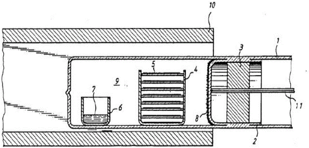
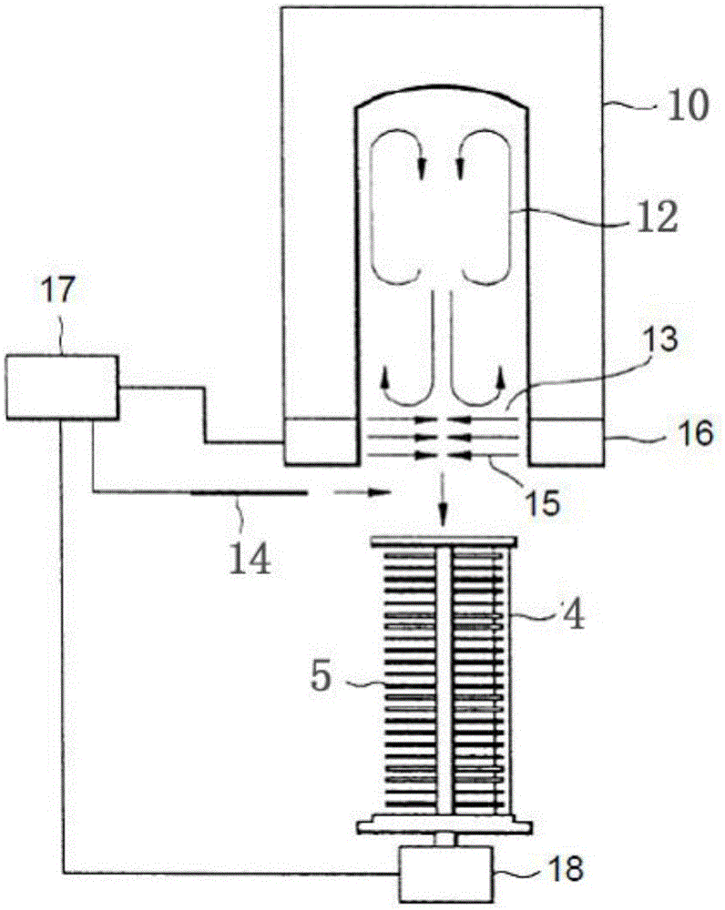
The invention relates to a diffusion chamber and a diffusion method used in process of producing semiconductor. A diffusion source is changed into a plane, parallel to a semiconductor sample, from points through a diffusion control device, namely, distances from the diffusion source to all areas of the sample are equal, the concentration degree and diffusion depth can be controlled, and the diffusion flux can be controlled in the semiconductor production process; the diffusion concentration and depth uniformity can be greatly improved, the concentration of source materials are evenly distributed in the semiconductor sample, and further the overall uniformity and yield of the sample can be greatly enhanced. The diffusion control device and a diffusion route thereof are close to the diffusion source (the source materials), once the source materials are volatilized, the diffusion control device can firstly play a blocking role, so that the lower surface of the diffusion control device is fast filled with the source material uniformly, then the source materials are redistributed by the diffusion route so as to uniformly arrive at all areas of the sample.

Description

technical field [0001] The invention relates to a method and device for dopant diffusion in the semiconductor manufacturing process, in particular to a method and device for controlling the diffusion process by controlling the diffusion path in the semiconductor manufacturing process. Background technique [0002] Over the past few decades, semiconductors have become important components in the electronics industry due to their miniaturization, light weight, multi-functionality and other characteristics. The modern electronics industry may require semiconductor devices with more specialized functions, such as semiconductor transistors, solar cells, light emitting diodes (LEDs), silicon controlled rectifiers, photodiodes, digital and analog integrated circuits. [0003] Photodiodes have been used in military, optical communications, information technology, and energy, among other fields. Photodiodes work by absorbing photons, or charged particles, and generating a current in...

Claims


Application Information

Patent Timeline
Patent Type & Authority Patents(China)
IPC IPC(8): C30B31/16H01L21/67
Inventor 叶瑾琳廖世蓉
Owner 浙江光特科技有限公司
Learn More