
Organic light emitting diode display

A technology of light-emitting diodes and displays, which is applied to static indicators, instruments, electric solid devices, etc., can solve the problems of brightness deviation, color deviation, and large change, and achieve the effect of improving color deviation defects

Active Publication Date: 2014-01-01
SAMSUNG DISPLAY CO LTD
View PDF4 Cites 17 Cited by
  • Summary
  • Abstract
  • Description
  • Claims
  • Application Information

AI Technical Summary

Problems solved by technology

[0006] However, the boost capacitor is generally set to have a smaller capacitance than the storage capacitor, so that the amount of variation according to process distribution is relatively large
Capacitance deviation among boost capacitors included in multiple pixels produces brightness deviation and color deviation

Method used


Image

  • Organic light emitting diode display
  • Organic light emitting diode display
  • Organic light emitting diode display

Examples


Embodiment Construction

[0034] Some embodiments will be described in detail below with reference to the accompanying drawings so that those skilled in the art to which the present invention pertains can easily carry out. As those skilled in the art would realize, the described embodiments may be modified in various different ways, all without departing from the spirit or scope of the present invention.

[0035] To clearly explain the present invention, parts irrelevant to the description are omitted, and the same or similar constituent elements are generally denoted by the same reference numerals throughout the specification.

[0036] In addition, the size and thickness of each configuration shown in the drawings are not limited thereto.

[0037] In the drawings, the thickness of layers, films, panels, regions, etc., may be exaggerated for clarity. In the drawings, the thicknesses of some layers and regions may be additionally shown for better understanding and ease of description. It will be under...


PUM


Abstract

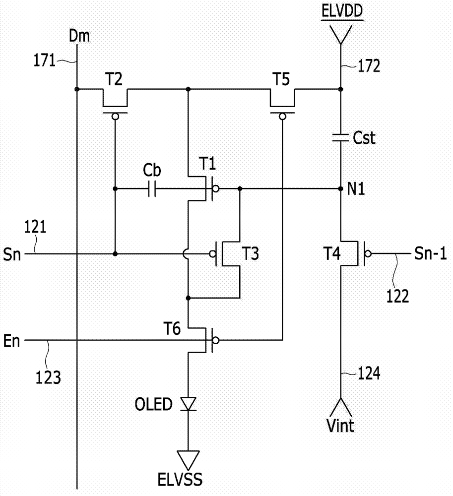
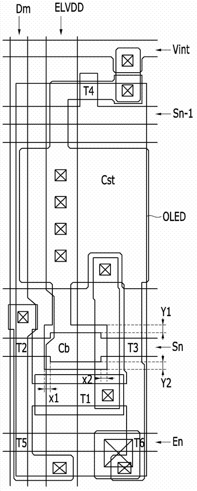
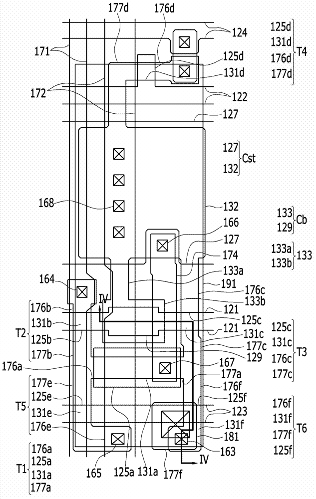
An organic light emitting diode (OLED) display includes a substrate; a scan line formed on the substrate and applying a scan signal; a data line and a driving voltage line intersecting the scan line and respectively applying a data signal and a driving voltage; a switching TFT connected to the scan line and data line; a driving TFT connected to a switching drain electrode of the switching TFT and the driving voltage line; an OLED connected to the driving drain electrode of the driving TFT; a storage capacitor connected between the driving voltage line and the driving gate electrode of the driving TFT; and a boosting capacitor including a first boosting capacitor plate connected to the driving gate electrode and a second boosting capacitor plate overlapping the first boosting capacitor plate and connected to the scan line, where an area of the first boosting capacitor plate of the boosting capacitor is larger than an area of the second boosting capacitor plate.

Description

technical field [0001] Broadly speaking, the described technology relates to organic light emitting diode (OLED) displays. Background technique [0002] An organic light emitting diode (OLED) display includes two electrodes and an organic emission layer disposed between the two electrodes. Electrons injected from one electrode and holes injected from the other electrode are combined in the organic emission layer to form excitons, and light is emitted by energy generated by the excitons. [0003] An organic light emitting diode (OLED) display includes a plurality of pixels including an organic light emitting diode (OLED) as a self-emitting element, and each pixel includes a capacitor and a plurality of thin film transistors (TFT) to drive the organic light emitting diode (OLED). [0004] The capacitor includes a storage capacitor that stores a data signal and a boost capacitor that performs a boosting operation according to a voltage change of the signal line to further corr...

Claims


Application Information

Patent Timeline
Patent Type & Authority Applications(China)
IPC IPC(8): H01L27/32G09G3/32
CPCH01L27/3265G09G3/32H01L27/32G09G2300/0819H10K59/1216G09G3/3233H10K59/352H10K59/131H10K50/805H10K50/814H10K50/824H10K50/844G09G3/3208
Inventor 洪相玟
Owner SAMSUNG DISPLAY CO LTD
Learn More