
Method for extracting trap time constant of gate dielectric layer of semiconductor device

A technology of time constant and gate dielectric layer, applied in semiconductor/solid-state device testing/measurement, instruments, electrical components, etc., can solve problems such as low efficiency, limited test time, and large difference in time constant magnitude

Active Publication Date: 2013-12-25
上海伦刻电子技术有限公司
View PDF3 Cites 3 Cited by
  • Summary
  • Abstract
  • Description
  • Claims
  • Application Information

AI Technical Summary

Problems solved by technology

For a certain gate voltage, there may be a situation where the two time constants have a large difference in magnitude, so the above method is limited by the test time and the storage capacity of the test instrument and it is difficult to realize; however, this situation is also an important research category. Therefore, it is necessary to realize the test of the trap time constant through other effective methods, especially to solve the above-mentioned problems, and then support the research on the trap behavior
In this regard, the current method basically obtains the occupancy probability of multiple time points through testing, and then fits the model to obtain the time constant; however, this method is inefficient, and a large amount of test data can meet certain accuracy requirements. Therefore, It is necessary to propose an efficient method for testing and extracting trap time constants that meets the accuracy requirements

Method used


Image

  • Method for extracting trap time constant of gate dielectric layer of semiconductor device
  • Method for extracting trap time constant of gate dielectric layer of semiconductor device
  • Method for extracting trap time constant of gate dielectric layer of semiconductor device

Examples


Embodiment Construction

[0029] Below by embodiment and in conjunction with accompanying drawing, describe testing method of the present invention in detail:

[0030] The test steps and data processing methods are as follows:

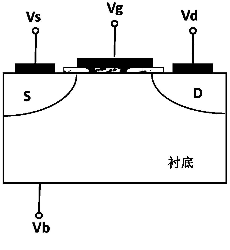
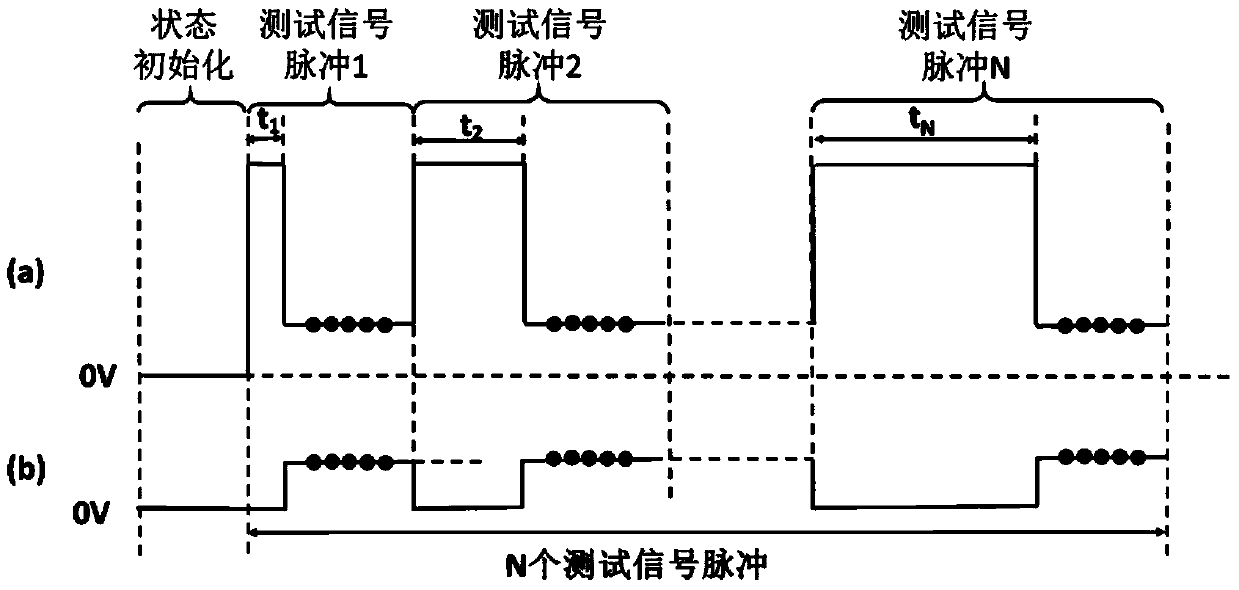
[0031] Test part (the test steps described below are the process of testing and extracting the capture time constant of the N-type device under the DC signal; the source terminal and the body terminal are both grounded during the test, that is, zero bias, probe A and probe B connected to gate terminal and drain terminal respectively):

[0032] 1) The purpose of this step is to initialize the state of the trap so that the trap is in an empty state before applying a high level signal. The drain terminal signal voltage is Vd0, and the gate terminal signal voltage is Vg0. Here, Vd0 and Vg0 are taken as ground signals, that is, zero bias, that is to say, it is necessary to ensure that the device is in a situation without any stress for a sufficient time. The purpose of this step is...


PUM


Abstract

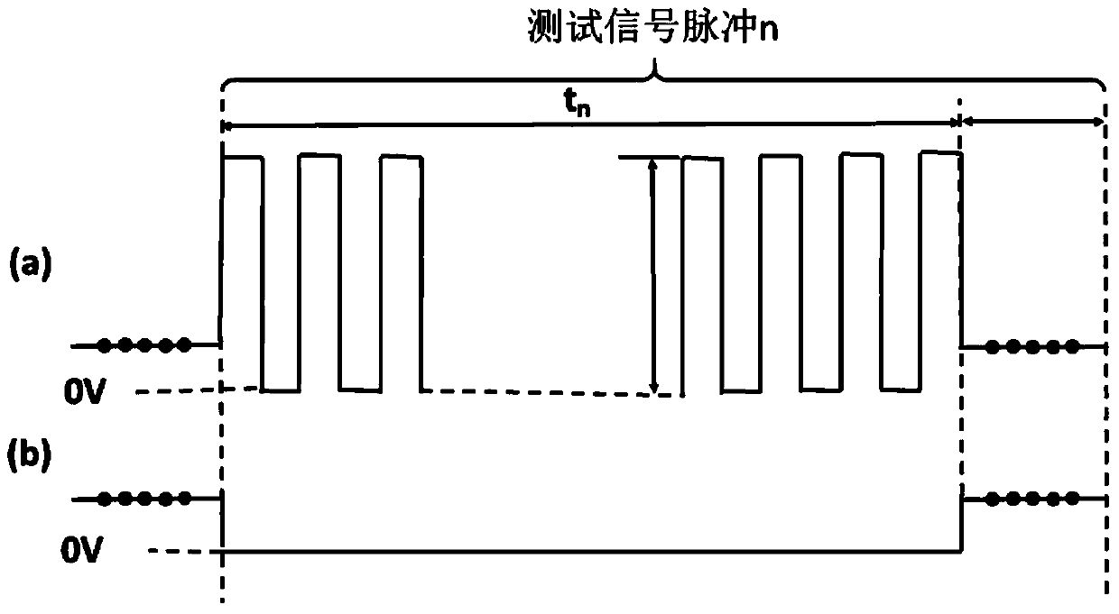
The invention discloses a method for extracting the trap time constant of a gate dielectric layer of a semiconductor device, belonging to the field of microelectronic device reliability. The method comprises the steps of firstly, initializing the trap state in the semiconductor device so that the final state of a trap is an empty state; then, applying a direct current (DC) signal or an alternating current (AC) signal to a gate terminal, and controlling a drain terminal to be zero-bias Vd1; after a period of time t1, respectively applying low voltage Vg2 and Vd2 onto the gate terminal and the drain terminal, and detecting the state of leak current Id; changing the time t1 to be t2 which is the sum of t1 and delta t, keeping other conditions unchanged, repeating the previous step under the condition that, and so on; after the measurement is carried out for N times, obtaining the current states of the drain terminal corresponding to the N time points t1, t1+ delta t,... t1+(N-1) delta t; finally, carrying out moving average and working out occupation probabilities P corresponding to (N-n) moment points; utilizing formula fitting to obtain the capture time constant and the launch time constant of the trap.

Description

technical field [0001] The invention belongs to the field of reliability of microelectronic devices, and relates to a method for extracting trap time constants in gate dielectric layers of small-scale semiconductor devices. Background technique [0002] With the gradual reduction of the scale of semiconductor devices, the number of traps in the gate dielectric layer is gradually reduced, which makes the random behavior of traps more and more attention, and the influence of electrical characteristics caused by a single trap in small-sized devices It is far greater than the impact of traps in large-scale devices; it will cause serious impacts in the circuit, for example, it will increase the delay of some logic circuits, and the read failure of static random access memory (SRAM), etc. Therefore, research on small-size The behavior of traps in devices, a comprehensive grasp of the basic characteristics of traps is of great significance for predicting the degradation characteris...

Claims


Application Information

Patent Timeline
Patent Type & Authority Applications(China)
IPC IPC(8): H01L21/66
CPCH01L22/14G01R31/2621G01N27/02G01R31/2601
Inventor 黄如郭少锋王润声任鹏鹏蒋晓波罗牧龙张兴
Owner 上海伦刻电子技术有限公司
Learn More