Novel latent fingerprint displaying method
A technology of latent fingerprints and fingerprints, which is applied in the field of electron beam evaporation metal films to show latent fingerprints, which can solve the problems of excessive thickness of the coating and restricting applications.
- Summary
- Abstract
- Description
- Claims
- Application Information
AI Technical Summary
Problems solved by technology
Method used
Image
Examples
Embodiment 1
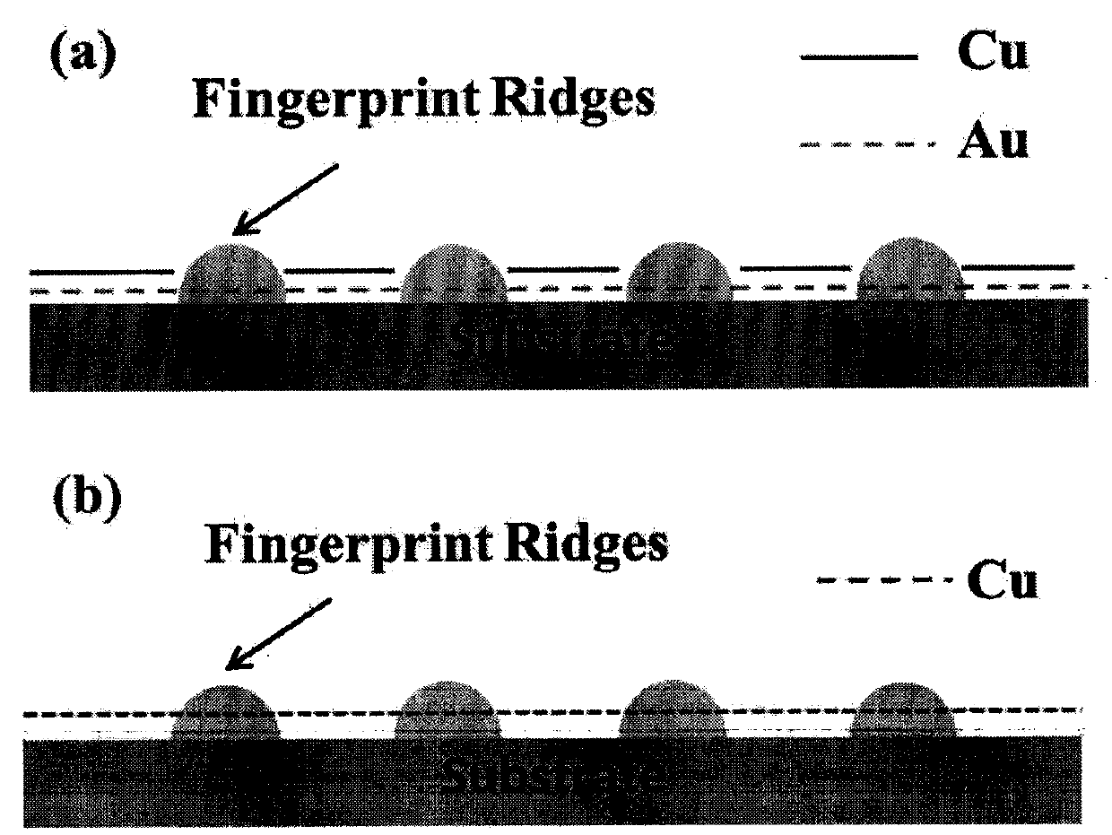
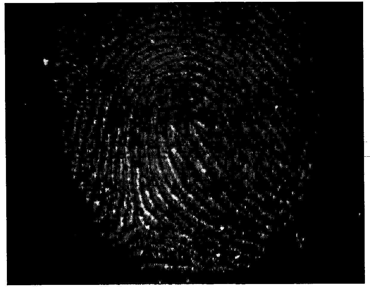
[0020] This embodiment provides a method of evaporating Cu (25nm) on a glass substrate to reveal 24h internal sweat latent fingerprints.
[0021] Step 1. Press the sweat submerged fingerprint on the glass substrate, put the sample into the vacuum chamber, put the copper target into the crucible at the same time, and close the vacuum chamber;
[0022] Step 2 Turn on the vacuum pump and pump the vacuum in the vacuum chamber to 10 -3 below pa. The substrate temperature is at room temperature, turn on the electron gun, and use electron beam to evaporate Cu;
[0023] Step 3: Open the baffle in front of the sample, the substrate temperature is at room temperature, start to deposit Cu film on the surface of the sample, use crystal controller to monitor the film thickness in real time, when the Cu film thickness is 25nm, close the baffle, and turn off the electron gun;
[0024] Step 4 Observe the fingerprint display effect from the observation window, turn off the vacuum pump, and f...
Embodiment 2
[0027] This embodiment provides a method for evaporating Au(5nm) / Cu(20nm) on a ceramic substrate to display sweat latent fingerprints left for 30 days.
[0028] Step 1: put the sample that was pressed on the ceramic substrate 30 days ago into the vacuum chamber, put the gold target and the copper target into the two crucibles at the same time, and close the vacuum chamber door;
[0029] Step 2 Turn on the vacuum pump and pump the vacuum in the vacuum chamber to 10 -3 Below pa, the substrate temperature is room temperature. First turn the crucible with the gold target under the electron gun, turn on the electron gun, evaporate the gold film with the electron beam, open the baffle in front of the sample, start depositing the gold film on the surface of the sample, and monitor the film thickness with an electronic crystal controller. When the film reaches 5nm, close the baffle in front of the sample and close the electron gun;
[0030] Step 3 Transfer the crucible with the copp...
PUM
| Property | Measurement | Unit |
|---|---|---|
| thickness | aaaaa | aaaaa |
Abstract
Description
Claims
Application Information
 - R&D
- Intellectual Property
- Life Sciences
- Materials
- Tech Scout
- Unparalleled Data Quality
- Higher Quality Content
- 60% Fewer Hallucinations
Browse by: Latest US Patents, China's latest patents, Technical Efficacy Thesaurus, Application Domain, Technology Topic, Popular Technical Reports.
© 2025 PatSnap. All rights reserved.Legal|Privacy policy|Modern Slavery Act Transparency Statement|Sitemap|About US| Contact US: help@patsnap.com


