
TM-polarization GaAsP/GaInP active-region 808nm quantum-well laser

An active region, quantum well technology, used in lasers, phonon exciters, laser components, etc., can solve problems such as unfavorable work, limited maximum output power level, and difficult growth.

Inactive Publication Date: 2013-12-18
Shandong Huaguang Optoelectronics Co. Ltd.
View PDF8 Cites 21 Cited by
  • Summary
  • Abstract
  • Description
  • Claims
  • Application Information

AI Technical Summary

Problems solved by technology

Patent CN1226759 reports a multi-quantum well laser. This structure couples multiple quantum wells through tunnel junctions to achieve the purpose of reducing optical power density in one structure, but this structure requires high growth technology and doping technology. And it is not easy to grow, and due to the mutual influence between multiple quantum wells, it is not conducive to work under the condition of high-power continuous current; with the development of technology, in order to obtain stable high-power output, it is currently necessary to reduce the large optical power density Cavity-wide waveguide structure has become a common structure for high-power lasers
Patent CN101820136A uses a large optical cavity and wide waveguide structure to achieve high-power light output, but the AlGaAs material with high aluminum composition limits the maximum output power level of the structure

Method used


Image

  • TM-polarization GaAsP/GaInP active-region 808nm quantum-well laser
  • TM-polarization GaAsP/GaInP active-region 808nm quantum-well laser
  • TM-polarization GaAsP/GaInP active-region 808nm quantum-well laser

Examples


Embodiment Construction

[0011] Technical scheme of the present invention is as follows:

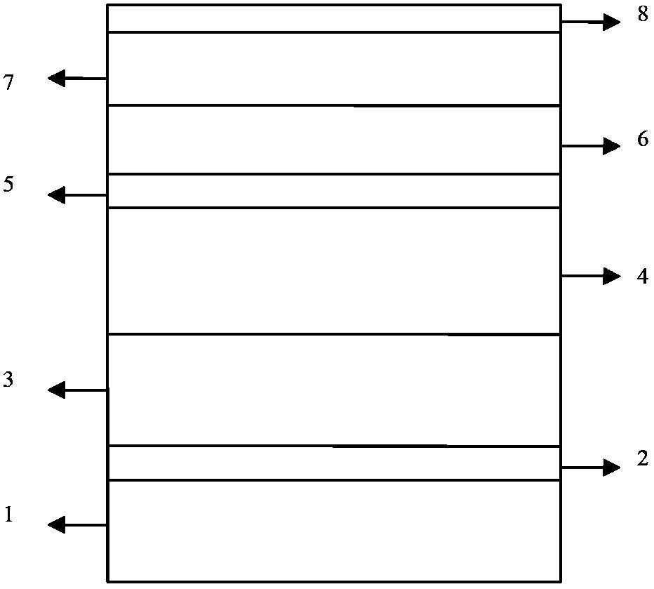
[0012] A TM polarized GaAsP / GaInP active region 808nm quantum well laser, including a substrate, a buffer layer, a lower confinement layer, a lower waveguide layer, a quantum well layer, an upper waveguide layer, an upper confinement layer and an ohmic contact arranged from bottom to top Floor;

[0013] The substrate is N-type highly doped gallium arsenic with the (100) plane offset to the (110) direction, and the off-angle is 0-15°. Preferably, according to the present invention, the N-type impurity in the substrate is Si, the doping concentration of Si is greater than 2×10 18 / cm 3 ;

[0014] The buffer layer is an N-type highly doped GaAs material with a thickness of 300-500nm. According to the present invention, preferably, the N-type impurity in the buffer layer is Si, and the doping concentration of Si is 1×10 18 / cm 3 ;

[0015] The lower limiting layer is an N-type aluminum gallium indium phosphide...


PUM

PropertyMeasurementUnit
Thicknessaaaaaaaaaa
Thicknessaaaaaaaaaa
Thicknessaaaaaaaaaa

Abstract

The invention provides a TM-polarization GaAsP / GaInP active-region 808nm quantum-well laser. The laser structurally comprises a substrate, a buffer layer, a type-N lower limit layer, a lower waveguide layer, a quantum well layer, an upper waveguide layer, a type-P upper limit layer, and an ohmic contact layer sequentially from bottom to top. The upper waveguide layer and the lower waveguide layer are made of aluminum-free material GaInP. The quantum well layer is made of GaAsP material. The waveguide layer and the quantum well layer form a wide-waveguide aluminum-free active region. The laser has the advantages that the influence of Al oxidization, growth interface roughness and accessory electric field at cavity surface upon the reliability in high power output, long service life and the like of the laser can be reduced effectively, the waveguide layer and the limit layers are optimally designed into wide-waveguide asymmetric structures, and internal loss can be reduced effectively, and maximum output power and reliability can be improved.

Description

technical field [0001] The invention relates to a TM polarized GaAsP / GaInP active region 808nm quantum well laser, which belongs to the technical field of semiconductor lasers. Background technique [0002] 808nm high-power quantum well lasers are widely used in the fields of pumping Nd:YAG solid-state lasers, industrial processing and laser medical treatment, and have very broad application prospects and market value. Due to the huge market demand, 808nm quantum well semiconductor lasers have been developed rapidly. With the development of applications, the output power requirements of lasers are increasing. For 808nm semiconductor lasers, the optical catastrophe damage of the cavity surface caused by high power density, and the temperature rise of the active region and cavity surface caused by the thermal effect of carrier recombination are the main factors that limit the maximum output optical power density. [0003] For more than ten years, with the development of lase...

Claims


Application Information

Patent Timeline
IPC IPC(8): H01S5/343H01S5/20
Inventor 李沛旭徐现刚张新蒋锴汤庆敏
Owner Shandong Huaguang Optoelectronics Co. Ltd.
Learn More