
A chip interface circuit pad driving method and device

A technology of an interface circuit and a driving method, applied in the field of electronic information, can solve the problems of increased inductance effect of the bonding wire, the chip cannot work normally, and the cost of the chip is increased, so as to reduce the cost of the chip, reduce the sso effect, and reduce the voltage change. Effect

Active Publication Date: 2016-09-28
SHENZHEN CHIPSBANK TECH
View PDF5 Cites 0 Cited by
  • Summary
  • Abstract
  • Description
  • Claims
  • Application Information

AI Technical Summary

Problems solved by technology

And because a chip includes multiple pads, when multiple pads need a large transient current to realize the level inversion of the received driving signal at the same time, multiple large transient currents will be generated, resulting in the state of the packaged chip. The inductance effect of the line is enhanced, which causes the voltage of the chip to change greatly, resulting in the sso (simultaneous switch output) effect, making the chip unable to work normally
[0004] At present, the inductance effect of the bonding wire of the packaged chip is reduced by increasing the number of power grounds connected to the chip to reduce the SSO effect. The same number of power ground pads and state wires of packaged chips will lead to an increase in the cost of the chip
[0005] It can be seen from the above that the existing technical solutions have the disadvantage of needing to increase the cost of the chip in order to reduce the sso effect

Method used


Image

  • A chip interface circuit pad driving method and device
  • A chip interface circuit pad driving method and device
  • A chip interface circuit pad driving method and device

Examples


Embodiment Construction

[0059] The following will clearly and completely describe the technical solutions in the embodiments of the application with reference to the drawings in the embodiments of the application. Apparently, the described embodiments are only some of the embodiments of the application, not all of them. Based on the embodiments in this application, all other embodiments obtained by persons of ordinary skill in the art without making creative efforts belong to the scope of protection of this application.

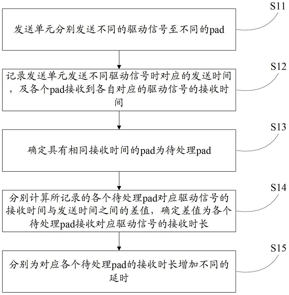
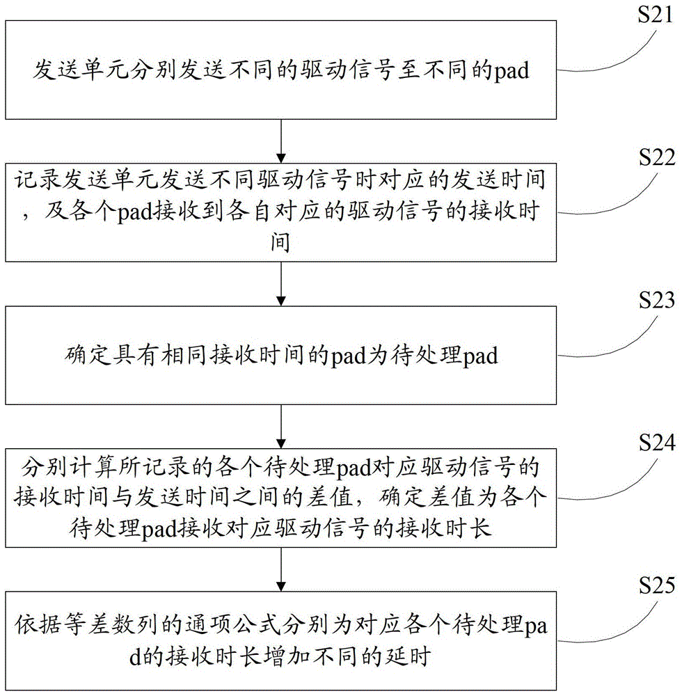
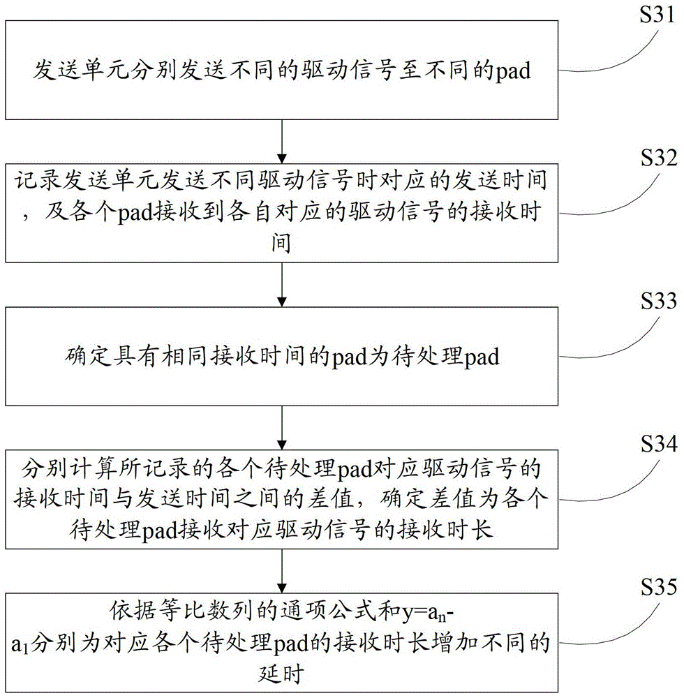
[0060] See figure 1 , which shows a flowchart of a chip interface circuit pad driving method provided by the present application, which may include the following steps:

[0061] Step S11: The sending unit sends different driving signals to different pads respectively.

[0062] In this embodiment, the sending unit is a part of the chip. The pad is the interface circuit of the chip. Since the chip includes a plurality of interface circuit pads of different chips, the sending unit of...


PUM


Abstract

The application provides a driving method for interface circuits pads of a chip, which comprises the following steps: sending different driving signals to different pads by a sending unit; recording corresponding sending time when the sending unit sends different driving signals, and receiving time when each pad receives a respective corresponding driving signal; defining pads with same receiving time as to-be-processed pads; respectively calculating difference values of the receiving time and the sending time of driving signals corresponding to each recorded to-be-processed pad, and defining the difference values as receiving durations when the each to-be-processed pad receives the corresponding driving signal; adding different time delay for the receiving durations corresponding to the each to-be-processed pad respectively to allow the corresponding receiving time of each to-be-processed pad to differ from one another, and to be different from receiving time of respective corresponding driving signals received by pads outside the to-be-processed pads; therefore, the sso effect can be alleviated without increasing the chip cost.

Description

technical field [0001] The present application relates to the field of electronic information, in particular to a chip interface circuit pad driving method and device. Background technique [0002] The chip is the carrier of the integrated circuit, and the interface circuit pad of the chip is a part of the chip, which is used to receive the driving signal sent by the chip to complete the signal interaction between the chip and the outside world. [0003] After the pad receives the driving signal sent by the chip, it needs a large transient current to realize the level inversion of the received driving signal, so as to realize the signal interaction between the chip and the outside world. And because a chip includes multiple pads, when multiple pads need a large transient current to realize the level inversion of the received driving signal at the same time, multiple large transient currents will be generated, resulting in the state of the packaged chip. The inductance effec...

Claims


Application Information

Patent Timeline
Patent Type & Authority Patents(China)
IPC IPC(8): H03K19/0175
Inventor 李华伟
Owner SHENZHEN CHIPSBANK TECH
Learn More