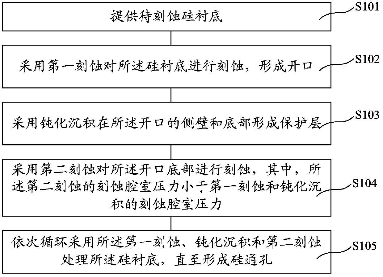
Through-silicon-via etching method
A through-silicon via and etching technology, which is applied in the fields of electrical components, semiconductor/solid-state device manufacturing, circuits, etc., can solve the problems of easy leakage and poor quality of through-silicon via interconnection structure, and achieve the effect of improving efficiency
- Summary
- Abstract
- Description
- Claims
- Application Information
AI Technical Summary
Problems solved by technology
Method used
Image

Examples
Embodiment Construction
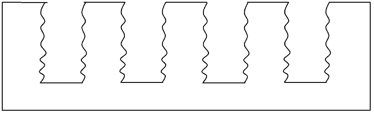
[0023] Research has been carried out on TSV products with serious leakage phenomena. After analyzing the cross-section of the TSV formed by the prior art with a scanning electron microscope, it is found that the morphology of the TSV formed by the existing process is as follows: figure 1 Shown is scalloped, serrated or corrugated to a greater degree, with higher roughness. Form an insulating layer on the surface of a shell-shaped, jagged or corrugated through-hole with high roughness, and then fill it with a conductive substance. The uniformity of the insulating layer is difficult to control, so that the conductive substance along the thinner position of the insulating layer Diffusion into the wafer, resulting in serious leakage of TSV products.
[0024] After further research on the process of forming the through-silicon vias, it was found that the reason for the formation of the surface of the above-mentioned corrugated through-holes is that in the formation process of the t...
PUM
| Property | Measurement | Unit |
|---|---|---|
| power | aaaaa | aaaaa |
| power | aaaaa | aaaaa |
| power | aaaaa | aaaaa |
Abstract
Description
Claims
Application Information
 - R&D
- Intellectual Property
- Life Sciences
- Materials
- Tech Scout
- Unparalleled Data Quality
- Higher Quality Content
- 60% Fewer Hallucinations
Browse by: Latest US Patents, China's latest patents, Technical Efficacy Thesaurus, Application Domain, Technology Topic, Popular Technical Reports.
© 2025 PatSnap. All rights reserved.Legal|Privacy policy|Modern Slavery Act Transparency Statement|Sitemap|About US| Contact US: help@patsnap.com