
Method for filling surface molecular layer defects of wide bandgap semiconductor adopting nano structure

A wide-bandgap semiconductor and nanostructure technology, applied in electrolytic capacitors, photovoltaic power generation, electrical components, etc., can solve problems such as low charge transfer recombination energy, low charge collection efficiency, and low activation energy.

Active Publication Date: 2013-11-13
CHANGCHUN INST OF APPLIED CHEMISTRY - CHINESE ACAD OF SCI
View PDF4 Cites 2 Cited by
  • Summary
  • Abstract
  • Description
  • Claims
  • Application Information

AI Technical Summary

Problems solved by technology

[0003] The purpose of the present invention is to improve the low charge transfer and recombination energy caused by the use of the current cobalt-based single-electron mediator, the activation energy of the reaction involved is small, and the charge collection efficiency during short circuit is reduced. Filling Method of Surface Molecular Layer Defects of Wide Bandgap Semiconductors

Method used


Image

  • Method for filling surface molecular layer defects of wide bandgap semiconductor adopting nano structure
  • Method for filling surface molecular layer defects of wide bandgap semiconductor adopting nano structure
  • Method for filling surface molecular layer defects of wide bandgap semiconductor adopting nano structure

Examples


Embodiment 1

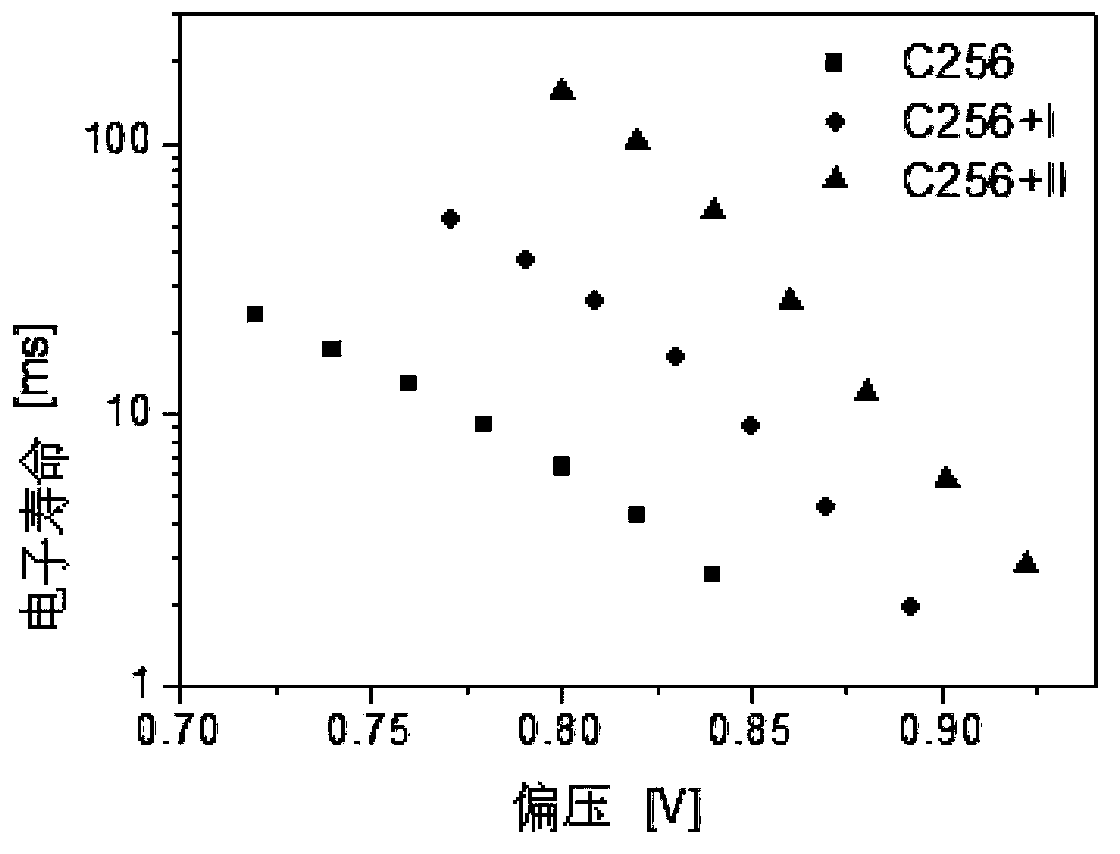
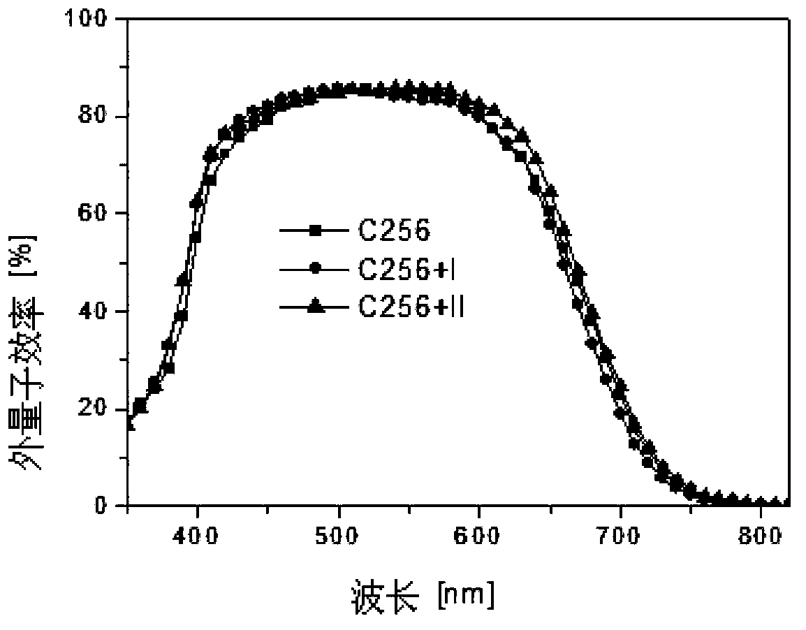
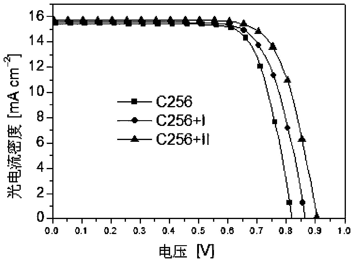
[0065] Soak the nanostructured titanium dioxide film electrode in the chlorobenzene solution containing 100 micromoles per liter of C256 dye for 12 hours for dyeing, then rinse with acetonitrile, and put the electrode into the solution containing 1 millimoles per liter of filler I or II was immersed in the acetonitrile solution for 5 minutes to fill the defects in the dye molecular layer.

[0066] The semiconductor electrode grafted with C256 dye and filler (I or II) was connected to the counter electrode covered with nano-platinum by using a 35-micron-thick thermal melting ring by means of heating and melting. The electrolyte is injected into the cavity between the two electrodes through the small hole on the counter electrode, and finally the small hole is heat-sealed with a hot-melt circular film and a cover glass to complete the preparation of the dye-sensitized solar cell. The electrolyte components are as follows: 0.25 moles per liter of tris(1,10-phenanthroline)cobalt(I...

Embodiment 2

[0069] Soak the nanostructured titanium dioxide film electrode in the chlorobenzene solution containing 100 micromoles per liter of C219 dye for 12 hours for dyeing, then rinse with acetonitrile, and put the electrode into the solution containing 1 millimoles per liter of filler I or II was immersed in the acetonitrile solution for 5 minutes to fill the defects in the dye molecular layer.

[0070] The semiconductor electrode grafted with C219 dye and filler (I or II) was connected to the counter electrode covered with nano-platinum by using a 35-micron thick thermal fusion ring by means of heating and melting. The electrolyte is injected into the cavity between the two electrodes through the small hole on the counter electrode, and finally the small hole is heat-sealed with a hot-melt circular film and a cover glass to complete the preparation of the dye-sensitized solar cell. The electrolyte components are as follows: 0.25 moles per liter of tris(1,10-phenanthroline)cobalt(II...

Embodiment 3

[0073] Soak the nanostructured titanium dioxide thin film electrode in the chlorobenzene solution containing 100 micromole per liter of C249 dye for 12 hours for dyeing, then rinse with acetonitrile, and put the electrode into the solution containing 1 millimole per liter of filler I or II was immersed in the acetonitrile solution for 5 minutes to fill the defects in the dye molecular layer.

[0074] The semiconductor electrode grafted with C249 dye and filler (I or II) was connected to the counter electrode covered with nano-platinum by using a 35-micron-thick thermal melting ring by means of heating and melting. The electrolyte is injected into the cavity between the two electrodes through the small hole on the counter electrode, and finally the small hole is heat-sealed with a hot-melt circular film and a cover glass to complete the preparation of the dye-sensitized solar cell. The electrolyte components are as follows: 0.25 moles per liter of tris(1,10-phenanthroline)cobal...


PUM


Abstract

The invention provides a method for filling surface molecular layer defects of a wide bandgap semiconductor adopting a nano structure, and effectively solves the problems that the interface charge composition is fast and the charge collecting efficiency is reduced during short-circuit due to the use of a cobalt-based single electron mediator with characteristics of low charge transfer reorganization energy and the like. The method comprises the steps as follows: an electrode of the wide bandgap semiconductor adopting the nano structure is soaked in a dye solution for dyeing; then a dyed semiconductor film is soaked in a solution containing a filling agent for filling the dye molecular layer defects; and the solubility of the dye in the solution containing the filling agent is smaller than 10 micromoles per litre. The invention further provides an application of the semiconductor electrode obtained with the method for filling the molecular layer defects of the wide bandgap semiconductor in dye-sensitized solar cells. According to the method for filling the surface molecular layer defects of the wide bandgap semiconductor adopting the nano structure, an electron tunneling distance of an interface composite reaction can be effectively controlled, so that the interface charge composition of the dye-sensitized solar cells is slowed down, and photovoltage, photocurrent and power conversion efficiency of a device can be improved.

Description

technical field [0001] The invention belongs to the field of wide bandgap semiconductors, in particular to a filling method for surface molecular layer defects of nanostructured wide bandgap semiconductors. Background technique [0002] Solar photovoltaic power generation is becoming an important technology for the world to meet the challenges of a low-carbon economy in the future. In order to reduce the cost of photovoltaic power generation and broaden its application fields, dye sensitization and organic solar cells have become the frontier and hot spot of current scientific research, and have attracted the attention of domestic and foreign industries. year 1991, etc. have made a major breakthrough in dye-sensitized solar cells (DSC) by using titanium dioxide thin films with large specific surface area and polypyridine ruthenium dyes with broad spectral response (Nature, 1991, 353, 373), and the global science and technology and industry circles began to seriously consid...

Claims


Application Information

Patent Timeline
IPC IPC(8): H01G9/04H01G9/042H01G9/20
CPCY02E10/542Y02E10/549
Inventor 张敏杨林王鹏
Owner CHANGCHUN INST OF APPLIED CHEMISTRY - CHINESE ACAD OF SCI
Learn More