Thin-film transistor device and method for manufacturing same, organic electroluminescent display elements and organic electroluminescent display device
A technology of thin-film transistors and components, applied in semiconductor/solid-state device manufacturing, transistors, electric solid-state devices, etc., can solve problems such as poor electrical connections
- Summary
- Abstract
- Description
- Claims
- Application Information
AI Technical Summary
Problems solved by technology
Method used
Image
Examples
Embodiment approach 1
[0127] 1. Overall structure of the organic EL display device 1
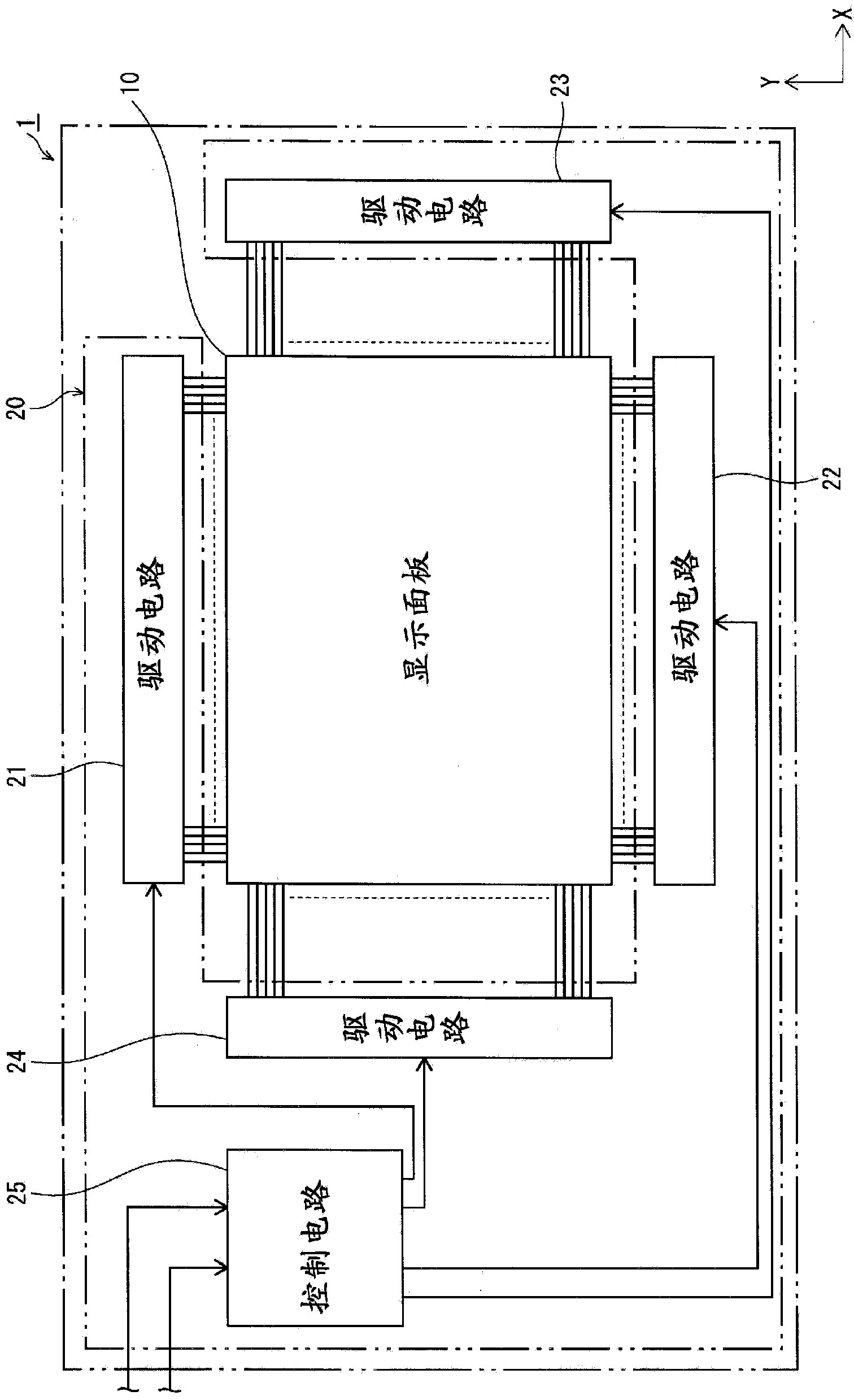
[0128] Below, use figure 1 The structure of the organic EL display device 1 according to Embodiment 1 of the present invention will be described.
[0129] Such as figure 1 As shown, the organic EL display device 1 is configured to include an organic EL display panel 10 and a drive control circuit unit 20 connected thereto.
[0130] The organic EL display panel 10 is a panel utilizing the electroluminescence phenomenon of organic materials, and is configured such that a plurality of organic EL elements are arranged in a matrix, for example. The drive control circuit unit 20 includes a control circuit 25 and four drive circuits 21 to 24 .
[0131] In the organic EL display device 1 according to this embodiment, the arrangement of the drive control circuit unit 20 with respect to the organic EL display panel 10 is not limited to this.
[0132] 2. Structure of the organic EL display panel 10
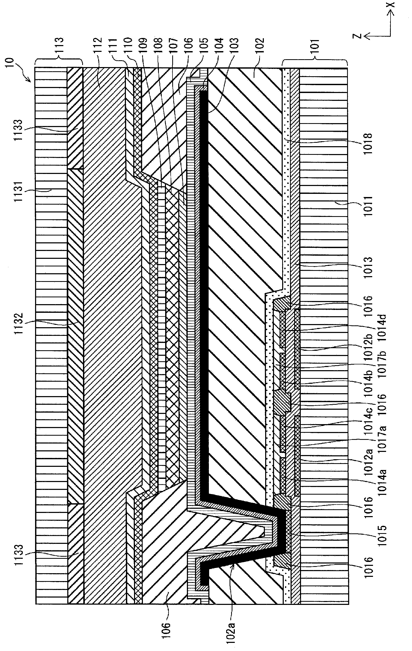
[0133] use fig...
Embodiment approach 2
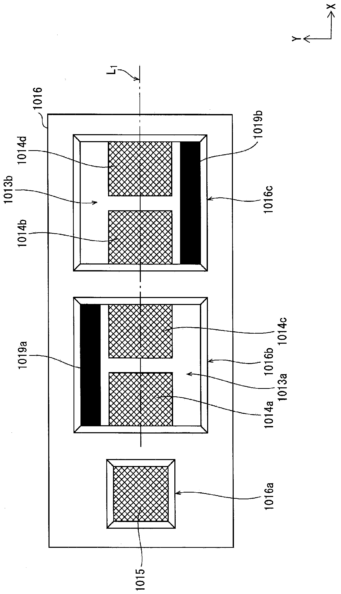
[0248] use Figure 9 (a) The structure of the TFT substrate according to Embodiment 2 of the present invention will be described. also, Figure 9 (a) is the same as that in Embodiment 1 above image 3 In the corresponding figures, other configurations are the same as those in Embodiment 1 described above, so illustration and description thereof will be omitted.
[0249] Such as Figure 9 As shown in (a), in the TFT substrate according to this embodiment, four openings 2016 a , 2016 b , 2016 c , and 2016 d are defined by the partition wall 2016 . Among them, the connection wirings 2015a and 2015d are arranged at the bottom of the openings 2016a and 2016d, respectively, and do not function as channel parts.
[0250] Furthermore, in this embodiment, if Figure 9 As shown in (a), neither the opening portion 2016a nor the opening portion 2016d functions as a channel portion, but one opening portion, for example, the opening portion 2016d belongs to the TFT element correspondin...
Embodiment approach 3
[0259] use Figure 9 (b) The structure of the TFT substrate according to Embodiment 3 of the present invention will be described. also, Figure 9 (b) is the same as that in Embodiment 1 above image 3 In the corresponding figures, other configurations are the same as those in Embodiments 1 and 2 described above, so illustration and description thereof are omitted.
[0260] Such as Figure 9 As shown in (b), in the TFT substrate according to this embodiment, the partition wall 2116 defines four openings 2116 a , 2116 b , 2116 c , and 2116 d . Among them, the connection wirings 2115a and 2115d are arranged at the bottom of the openings 2116a and 2116d, respectively, and do not function as channel parts.
[0261] Furthermore, in this embodiment, if Figure 9 As shown in (b), neither the opening portion 2116a nor the opening portion 2116d functions as a channel portion, but one opening portion, for example, the opening portion 2116d belongs to the TFT element corresponding to...
PUM
 Abstract
Description
Claims
Application Information
 - R&D
- Intellectual Property
- Life Sciences
- Materials
- Tech Scout
- Unparalleled Data Quality
- Higher Quality Content
- 60% Fewer Hallucinations
Browse by: Latest US Patents, China's latest patents, Technical Efficacy Thesaurus, Application Domain, Technology Topic, Popular Technical Reports.
© 2025 PatSnap. All rights reserved.Legal|Privacy policy|Modern Slavery Act Transparency Statement|Sitemap|About US| Contact US: help@patsnap.com


