ingaas/gaas infrared detector with wide detection band
A technology of infrared detectors and bands, applied in semiconductor devices, electrical components, circuits, etc., can solve problems such as lattice mismatch and detector performance degradation, and achieve improved detection rate, suppressed dark current, and reduced surface recombination Effect
- Summary
- Abstract
- Description
- Claims
- Application Information
AI Technical Summary
Problems solved by technology
Method used
Image
Examples
Embodiment
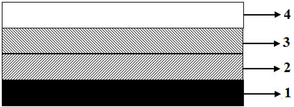
[0030] Step 1. First grow a layer of about 100 nm Si doping concentration of 2×10 on the S-doped n-type GaAs substrate 1 at a temperature of 450° C. by using the MOCVD system. 18 cm -3 InAs 0.60 P 0.40 Buffer layer 2, then raise the temperature to 580°C, during the heating process InAs 0.60 P 0.40 The buffer layer 2 is annealed and recrystallized to release the stress caused by the lattice mismatch and become the interface for the next growth. The thickness of the buffer layer 2 is 1 μm;
[0031] Step 2: After keeping the temperature at 550° C. for 3-5 minutes, grow a layer of 3 μm Si doping concentration on the above interface with a doping concentration of 8×10 16 cm -3 n-type In 0.82 Ga 0.18 As absorption layer 3;
[0032] Step 3, growing a Be doping concentration of 1 μm on the absorber layer 3 with a concentration of 2×10 17 cm -3 p-type In 0.82 Al 0.18 The As cap layer 4 is used to obtain an InGaAs / GaAs infrared detector with a pin structure and a wide detect...
PUM
 Abstract
Description
Claims
Application Information
 - R&D
- Intellectual Property
- Life Sciences
- Materials
- Tech Scout
- Unparalleled Data Quality
- Higher Quality Content
- 60% Fewer Hallucinations
Browse by: Latest US Patents, China's latest patents, Technical Efficacy Thesaurus, Application Domain, Technology Topic, Popular Technical Reports.
© 2025 PatSnap. All rights reserved.Legal|Privacy policy|Modern Slavery Act Transparency Statement|Sitemap|About US| Contact US: help@patsnap.com

