Wire method

A wire bonding and wire bonding technology, which is applied in the direction of semiconductor devices, electrical components, circuits, etc., can solve the problems of difficult to control plastic materials, failure, etc., and achieve the effect of improving the production process yield and avoiding the effect of bonding wires touching each other and shorting out

Active Publication Date: 2016-06-15
NAN YA TECH
View PDF3 Cites 0 Cited by
  • Summary
  • Abstract
  • Description
  • Claims
  • Application Information

AI Technical Summary

Problems solved by technology

In this way, not only is it difficult to control the shape of the plastic material 20 coating, but also it is easy to wrap air bubbles in the plastic material 20
In addition, the air bubbles in the plastic material 20 will cause delamination and failure of the package during the subsequent reliability test.

Method used


Image

  • Wire method
  • Wire method
  • Wire method

Examples


Embodiment Construction

[0020] In order to make the purpose and features of the present invention more obvious and understandable, the specific implementation manners of the present invention will be further described below in conjunction with the accompanying drawings.

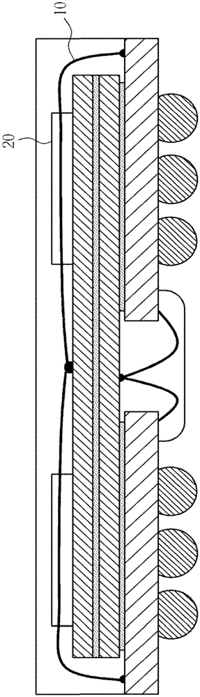
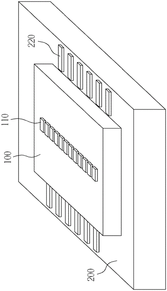
[0021] Please refer to Figure 2-4 , is a three-dimensional schematic diagram of a wire bonding method according to an embodiment of the present invention. Such as figure 2 As shown, the chip 100 is placed on the carrier 200 . The chip 100 has wire bonding pads 110 , and the carrier 200 has pins 220 . Such as image 3 As shown, the plastic material 20 is dispensed (and attached) on the chip 100 , and is located between the bonding pad 110 and the lead 220 . The plastic material 20 is a polymer material, preferably a polymer material with high viscosity and high thixotropy. Next, if Figure 4 As shown, the bonding wire 30 is bonded on the bonding pad 110 and the lead 220 , the bonding wire 30 is connected between the bonding p...


PUM


Abstract

The invention discloses a wire bonding method, comprising: (1) placing a chip on a carrier; (2) pointing a plastic material on the chip, wherein the plastic material is located at the wire bonding of the chip between the pad and the pins of the carrier; (3) wire bonding on the bonding pad and the pins, so that the bonding wires are connected between the bonding pads and the pins, and buried into the plastic material. The wire bonding method proposed by the present invention can immediately embed and fix the bonding wires by plastic materials during the bonding process, thus avoiding the mutual collision and short circuit of the bonding wires caused by vibration during the bonding process, and improving the manufacturing process. yield.

Description

technical field [0001] The invention relates to a wire bonding method, in particular to a wire bonding method for embedding welding wires into plastic materials. Background technique [0002] With the development of electronic structures towards high capacity, high density and light weight, more functional requirements and more output / input numbers must be met in a smaller volume. When the size of the chip's bonding pad and The spacing is designed to be smaller, and the wire bonding must also choose a thinner wire. At present, the most commonly used 0.9 (mil, thousandth inch) bonding wire in the industry can no longer be used on the bonding pad of chips below 50×50 (um, micron), 0.8 (mil, thousandth inch) The following wire bonding has gradually become the mainstream of today's wire bonding process. [0003] However, small-diameter soldering wires are a big challenge for long-distance bonding. The smaller the wire diameter, the lighter and softer the welding wire is. Duri...

Claims


Application Information

Patent Timeline
Patent Type & Authority Patents(China)
IPC IPC(8): H01L21/60
CPCH01L2224/4824H01L2224/48465H01L2224/48471H01L2224/48479H01L2224/48991H01L2224/73265H01L2224/78301H01L2224/85051H01L2224/85186H01L2924/15311H01L24/78H01L2924/00014H01L2224/78H01L2924/181H01L2924/10161H01L2224/85H01L2924/00H01L2924/00012H01L2224/4554
Inventor 陈逸男徐文吉叶绍文刘献文
Owner NAN YA TECH
Why Eureka
Try Eureka