Device used for attaching chip-on-film to panel and using method thereof

A chip-on-film and panel technology is applied in the direction of using optical devices, lamination devices, measuring devices, etc., and can solve problems such as adverse effects on product quality, deviation of the attachment of the chip-on film 120, and bending of the panel 140, so as to avoid artificial Operational errors, reduced bending, improved quality effects

Inactive Publication Date: 2013-10-09
TCL CHINA STAR OPTOELECTRONICS TECH CO LTD
View PDF6 Cites 3 Cited by
  • Summary
  • Abstract
  • Description
  • Claims
  • Application Information

AI Technical Summary

Problems solved by technology

When the indenter 110 presses down, the gap 160 will cause the panel 140 to bend, thereby causing the chip-on-film 120 to be attached to a deviation, which will adversely affect the quality of the product

Method used


Image

  • Device used for attaching chip-on-film to panel and using method thereof
  • Device used for attaching chip-on-film to panel and using method thereof
  • Device used for attaching chip-on-film to panel and using method thereof

Examples


Embodiment Construction

[0022] The present invention will be further described below in conjunction with accompanying drawing.

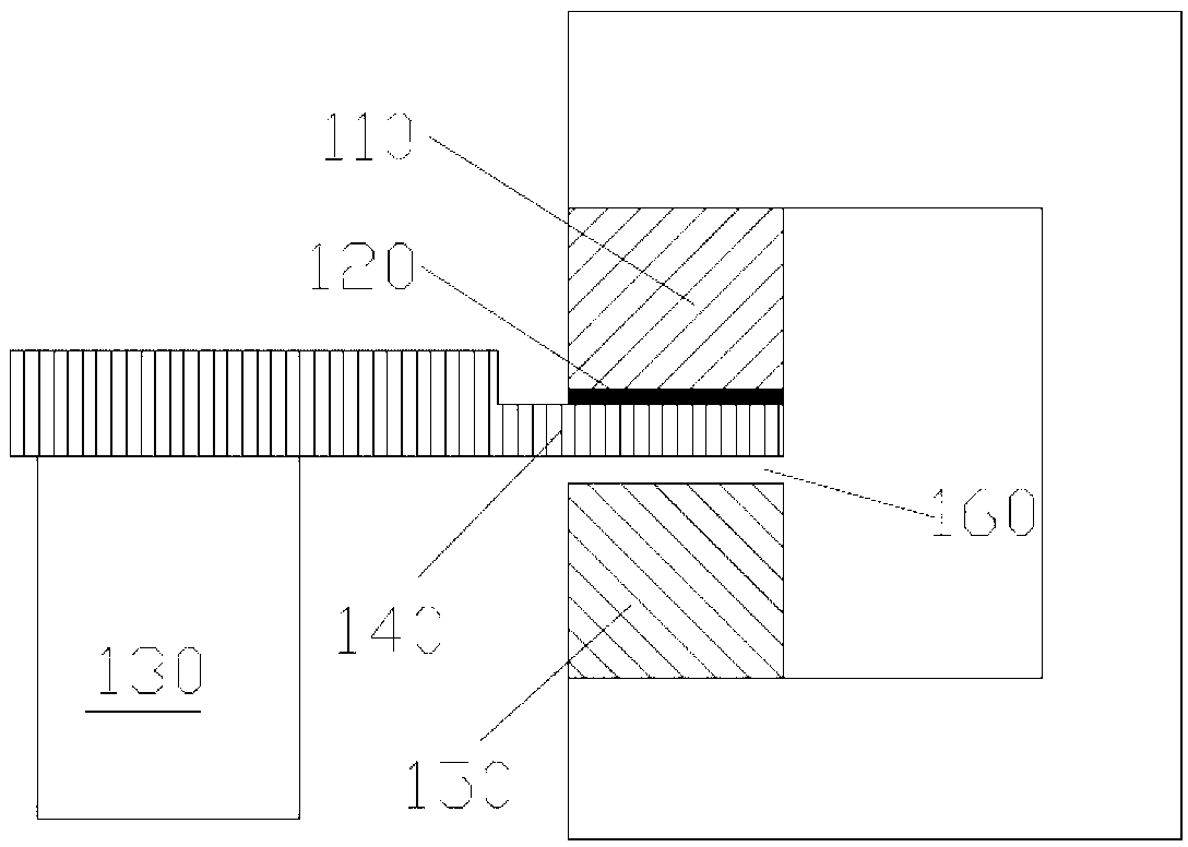
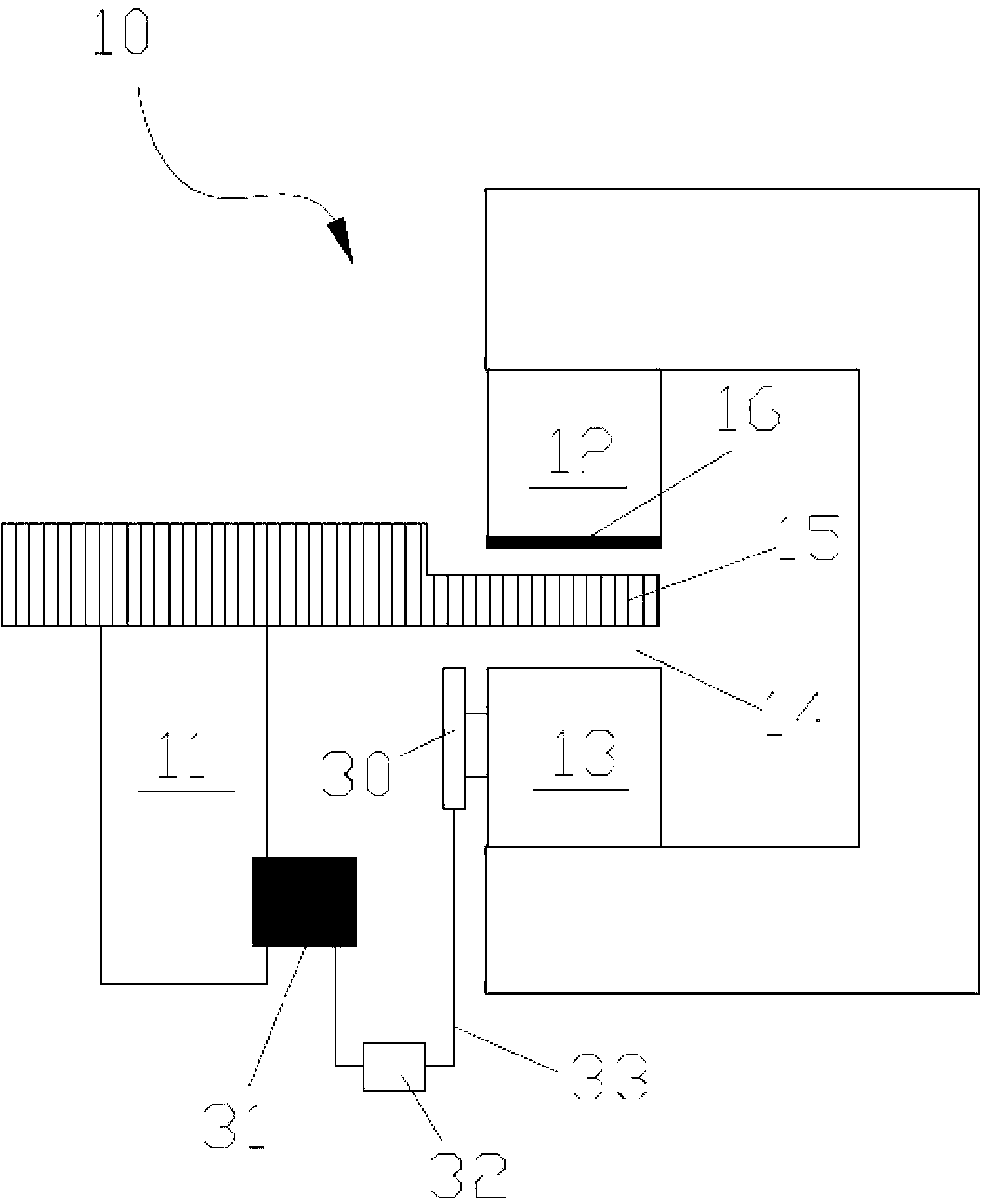
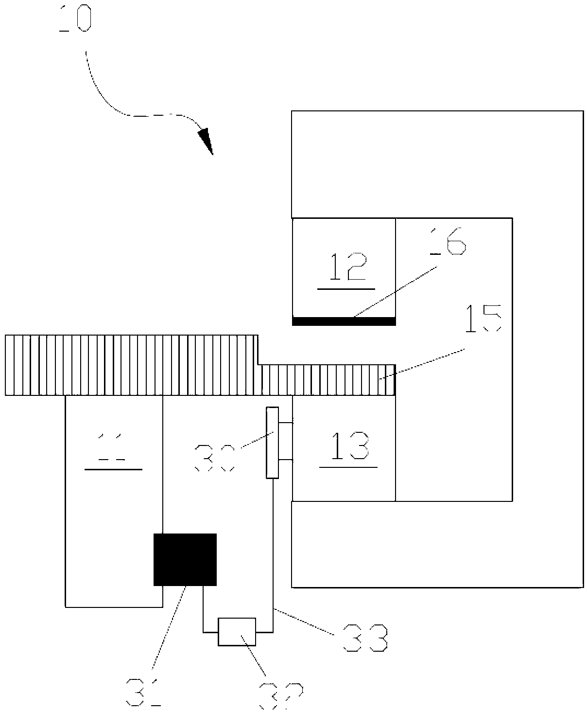
[0023] figure 2 A device 10 for attaching a chip-on-film to a panel according to the present invention (hereinafter referred to as device 10 ) is schematically shown. The device 10 includes a platform 11 , a pressure head 12 , a support mechanism 13 used in conjunction with the pressure head 12 (for example, the pressure head 12 and the support mechanism 13 are facing each other.) and a distance adjustment mechanism. Among them, the platform 11 is used to transport the panel 15, the indenter 12 is used to carry the chip-on-chip film 16, and the distance adjustment mechanism is used to measure the relationship between the panel 15 and the support mechanism 13 after the panel 15 is sent between the indenter 12 and the support mechanism 13. and reduce the distance between them. Of course, the device 10 also includes other components, which are well known to those skilled in...


PUM


Abstract

The invention relates to a device used for attaching a chip-on-film to a panel and a using method thereof. The device used for attaching the chip-on-film to the panel comprises a platform used for conveying the panel, a pressing head used for carrying the chip-on-film, a panel supporting mechanism which is matched with the pressing head for use, and a distance adjusting mechanism which is used for measuring and reducing the distance between the panel and the supporting mechanism after the panel is conveyed to a position between the pressing head and the supporting mechanism. The device used for attaching the chip-on-film to the panel has the advantages that the distance between the panel and the supporting mechanism can be reduced, attaching deviation of the chip-on-firm is avoided, and the quality of products is improved.

Description

technical field [0001] The invention relates to the field of liquid crystal module manufacturing, in particular to a device for attaching a chip-on-chip film to a panel. The invention also relates to methods of using such devices. Background technique [0002] The liquid crystal panel includes a panel (Lead) and a chip-on-chip attached to the panel. The thickness of the chip-on-film is very small, and it is usually called chip-on-film (COF). In order to attach the COF on the panel, a COF attaching device is usually used, figure 1 A schematic diagram of a prior art device for attaching a chip-on-film to a panel is shown. [0003] In the process of attaching the COF to the panel, firstly, the pressure head 110 absorbs the COF 120 . Next, the panel 140 is moved to the position of the indenter 110 through the servo platform 130 , and a supporting mechanism 150 is provided directly below the panel 140 for supporting. Through the cooperation of the pressure head 110 and the s...

Claims


Application Information

Patent Timeline
Patent Type & Authority Applications(China)
IPC IPC(8): G02F1/1333B32B37/00
CPCG02F1/1303H05K2201/10128G01B11/026H05K3/0058H05K2201/10681Y10T29/49004Y10T29/53178
Inventor 陈方甫
Owner TCL CHINA STAR OPTOELECTRONICS TECH CO LTD
Why Eureka
Try Eureka