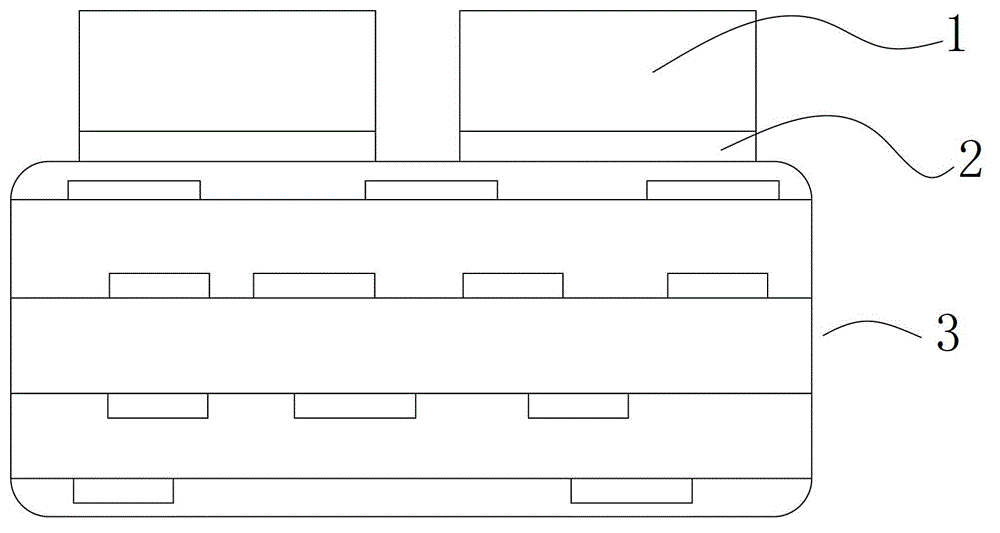
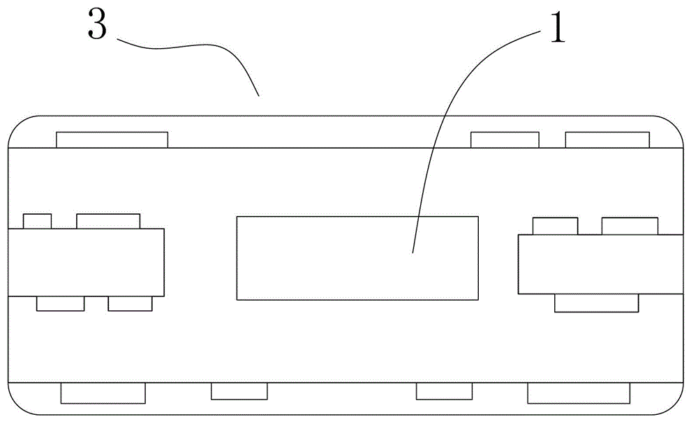
Circuit board with large current module and manufacturing method for circuit board
A manufacturing method and high-current technology, which are applied to printed circuits connected to non-printed electrical components and assembling printed circuits with electrical components, can solve the problems of space occupation, quality and reliability and safety hazards, and achieve the purpose of preventing flashbacks. and the effect of the broken drill bit
- Summary
- Abstract
- Description
- Claims
- Application Information
AI Technical Summary
Problems solved by technology
Method used
Image
Examples
Embodiment 1
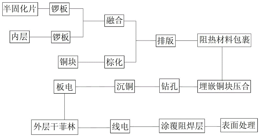
[0085] A method for making a circuit board with a large current module, such as figure 2 shown, including the following steps:
[0086] 1) Inner layer and prepreg gong board and fusion: firstly pre-stretch the inner layer and prepreg according to 0.3 mil / inch (mil / inch) in the radial direction and 0.5 mil / inch (mil / inch) in the weft direction, and perform gong Then according to the conventional process, the finished prepreg (5 pieces of prepreg of model 7628) and the inner layer (2 pieces of inner layer with a thickness of 21mil) are fused and combined, fixed with rivets, and then according to the predetermined design graphics. The embedding space of the copper block is provided on the layer and the prepreg. Among them, 1mil is 25.4μm.
[0087] 2) Embedding of high-current modules: First, the corners of the copper block are rounded and chamfered, and then browned. The browning parameters are: sodium hypochlorite concentration 4.2%, hydrogen peroxide concentration 4%, temper...
Embodiment 2
[0098] The manufacturing method of the circuit board with a large current module in this embodiment is basically the same as that in Embodiment 1, except that:
[0099] 1) Inner layer and prepreg gong board and fusion: first, the inner layer and prepreg are pre-stretched according to 0.2 mil / inch (mil / inch) in the radial direction and 0.4 mil / inch (mil / inch) in the weft direction.
[0100] 2) Embedding of high-current modules: Browning treatment parameters are: sodium hypochlorite concentration 3.8%, hydrogen peroxide concentration 3.3%, temperature 32°C and etching rate 1.25μm / cm 2 . When carrying out the embedding copper block pressing step, the pressing temperature and pressing plate pressure are carried out according to the parameters in Table 3 below.
[0101] Table 3. Lamination parameters of embedded copper block
[0102]
[0103]
[0104] At the beginning, the system was evacuated for 5 minutes to make the vacuum degree less than 20mbar. After maintaining for 150...
Embodiment 3
[0110] The manufacturing method of the circuit board with a large current module in this embodiment is basically the same as that in Embodiment 1, except that:
[0111] 1) Inner layer and prepreg gong board and fusion: first, the inner layer and prepreg are pre-stretched according to 0.4 mil / inch (mil / inch) in the radial direction and 0.6 mil / inch (mil / inch) in the weft direction.
[0112] 2) Embedding of high-current modules: Browning treatment parameters are: sodium hypochlorite concentration 4.6%, hydrogen peroxide concentration 5%, temperature 38°C and etching rate 1.75μm / cm 2 . When carrying out the embedding copper block pressing step, the pressing temperature and pressing plate pressure are carried out according to the parameters in Table 5 below.
[0113] Table 5. Embedded copper block pressing parameters
[0114]
[0115] At the beginning, the system was evacuated for 5 minutes to make the vacuum degree less than 20mbar. After maintaining for 100 minutes, the vac...
PUM
 Abstract
Description
Claims
Application Information
 - R&D
- Intellectual Property
- Life Sciences
- Materials
- Tech Scout
- Unparalleled Data Quality
- Higher Quality Content
- 60% Fewer Hallucinations
Browse by: Latest US Patents, China's latest patents, Technical Efficacy Thesaurus, Application Domain, Technology Topic, Popular Technical Reports.
© 2025 PatSnap. All rights reserved.Legal|Privacy policy|Modern Slavery Act Transparency Statement|Sitemap|About US| Contact US: help@patsnap.com


