Method for measuring the removal amount of the bottom metal layer of the contact hole

A bottom metal layer and contact hole technology, which is applied in the field of semiconductors, can solve the problems of hidden product quality, large distortion and error of results, and large distortion and error, and achieve the effects of saving manpower, stabilizing resistance value and electrical characteristics

Active Publication Date: 2016-03-02
SHANGHAI HUALI MICROELECTRONICS CORP
View PDF4 Cites 0 Cited by
  • Summary
  • Abstract
  • Description
  • Claims
  • Application Information

AI Technical Summary

Problems solved by technology

[0005] However, relying on the removal amount of the bottom metal layer obtained by the electronic transmission scanner and measuring the result by PCI software has a large degree of distortion and error, which cannot meet the needs of the actual process
More seriously, due to the large distortion and error of the results obtained by relying on the electronic transmission scanner, there are indirect errors in the debugging of the etching time to a certain extent, which has a great hidden danger to the product quality

Method used


Image

  • Method for measuring the removal amount of the bottom metal layer of the contact hole
  • Method for measuring the removal amount of the bottom metal layer of the contact hole
  • Method for measuring the removal amount of the bottom metal layer of the contact hole

Examples


Embodiment Construction

[0021] In order to illustrate the technical content, structural features, achieved goals and effects of the present invention in detail, the following will be described in detail in conjunction with the embodiments and accompanying drawings.

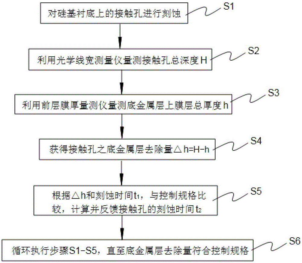
[0022] see figure 1 , figure 1 Shown is a flow chart of the method for measuring the removal amount of the bottom metal layer of the contact hole according to the present invention. The method for measuring the removal amount of the bottom metal layer of the contact hole includes:

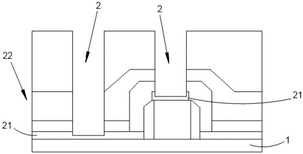
[0023] Executing step S1: etching the contact hole provided on the silicon-based substrate;

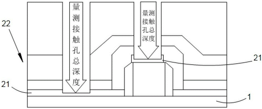
[0024] Executing step S2: measuring the total depth H of the contact hole by using an optical line width measuring instrument;

[0025] Executing step S3: measuring the total thickness h of the film layer on the bottom metal layer of the contact hole by using the front-layer film thickness measuring instrument;

[0026] Execute step S4: obtain the removal amount ...


PUM


Abstract

A measuring method for the removing amount of a bottom metal layer of a contact hole comprises the following steps: S1, etching the contact hole; S2, measuring the total depth H of the contact hole by using an optical line width measuring instrument; S3, measuring the total thickness h of a film layer positioned on the bottom metal layer by using a front layer film thickness measuring instrument; S4, obtaining the removing amount of the bottom metal layer of the contact hole through the formula: Delta h=H-h. According to the invention, the optical line width measuring instrument is used for obtaining the removing amount Delta h of the bottom metal layer of the contact hole, the relationship between electrical property and resistance value is used for judging whether the removing amount Delta h of the bottom metal layer of the contact hole conforms to a control specification, etching time of the contact hole can be fed back and adjusted quickly and timely in an on-line manner, the removing amount of the bottom metal layer of the on-line product contact hole can be precisely controlled and stabilized, and the stable resistance value and electric characteristic can be obtained, so that manpower and material resources are greatly saved, and the removing amount of the bottom metal layer of the contact hole can be precisely controlled.

Description

technical field [0001] The invention relates to the technical field of semiconductors, in particular to a method for measuring the removal amount of a bottom metal layer of a contact hole. Background technique [0002] In the process technology of 65nm and below, in order to improve the electrical contact of the circuit and improve the overall performance of the circuit, the removal amount control of the bottom metal layer of the contact hole is very important. [0003] Usually, because the etching area of ​​the contact hole is small, the general etching program is not realized by signal capture, but by the etching time. Therefore, for problems such as contact hole etching and etching, the bottom metal layer of the contact hole must have a certain amount of removal, so as to ensure the safety of the contact hole etching. However, the removal amount of the bottom metal layer must be strictly defined and controlled. Once the specification control is exceeded, the depth of the...

Claims


Application Information

Patent Timeline
Patent Type & Authority Patents(China)
IPC IPC(8): H01L21/66
Inventor 张志豪张颂周荆泉任昱吕煜坤张旭升
Owner SHANGHAI HUALI MICROELECTRONICS CORP
Why Eureka
Try Eureka