Grapheme field effect transistor and preparation method thereof
A field-effect transistor and graphene technology, which is applied in semiconductor/solid-state device manufacturing, semiconductor devices, electrical components, etc., can solve the problems of device performance degradation, reduce carrier mobility, etc., and achieve high dielectric constant and good top The effect of gate modulation capability and simple fabrication process
- Summary
- Abstract
- Description
- Claims
- Application Information
AI Technical Summary
Problems solved by technology
Method used
Image
Examples
preparation example Construction
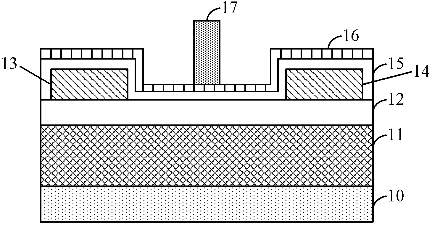
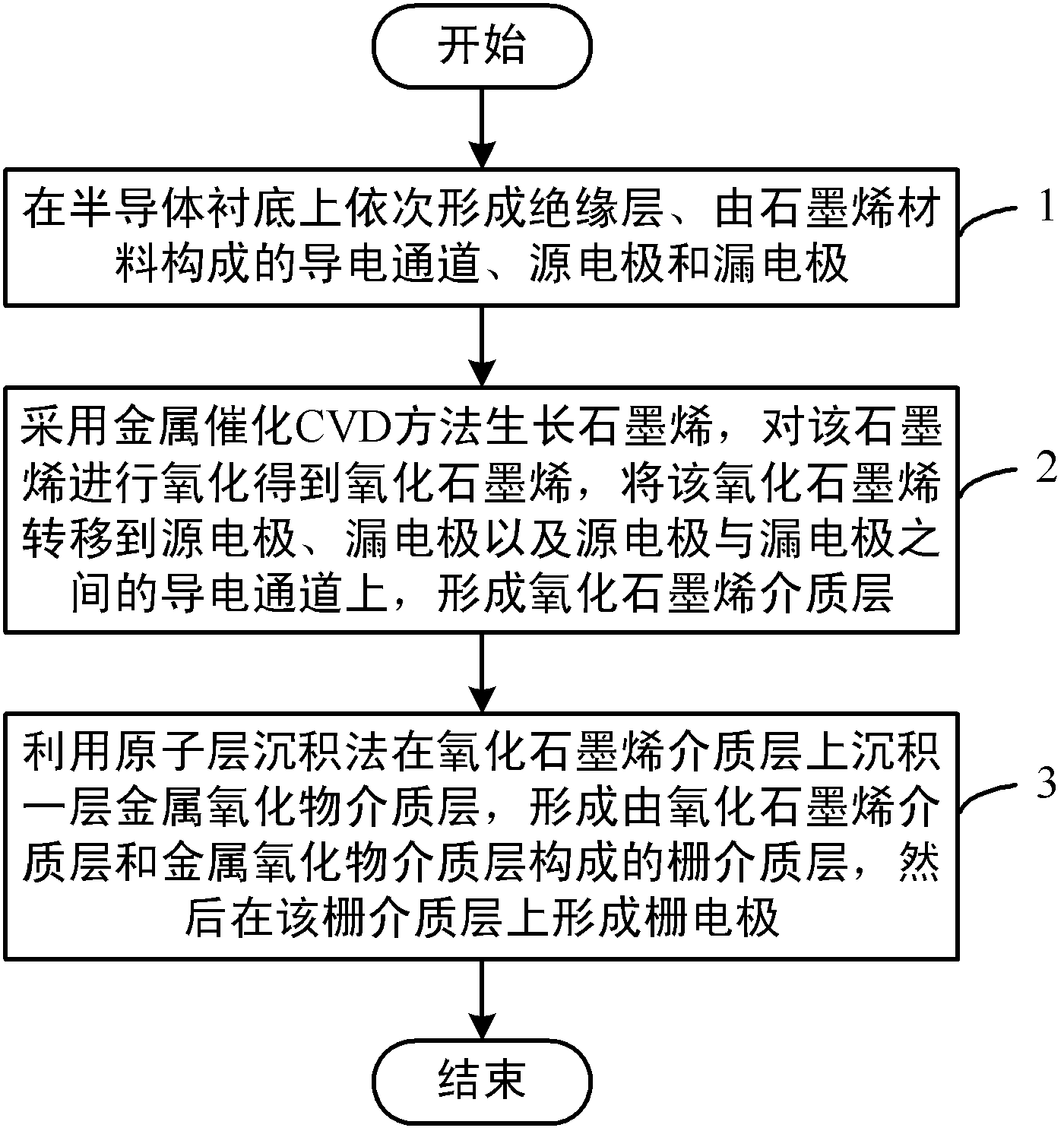
[0027] figure 2 It is prepared according to the embodiment of the present invention figure 1 The method flowchart of the shown graphene field effect transistor, the method may further comprise the steps:
[0028] Step 1: sequentially forming an insulating layer, a conductive channel made of graphene material, a source electrode and a drain electrode on the semiconductor substrate;
[0029] Step 2: grow graphene by metal-catalyzed CVD method, oxidize the graphene to obtain graphene oxide, transfer the graphene oxide to the source electrode, the drain electrode and the conductive channel between the source electrode and the drain electrode to form an oxide Graphene dielectric layer;
[0030] Step 3: Deposit a metal oxide dielectric layer on the graphene oxide dielectric layer by atomic layer deposition to form a gate dielectric layer composed of a graphene oxide dielectric layer and a metal oxide dielectric layer, and then on the gate dielectric layer A gate electrode is for...
Embodiment 1
[0033] Embodiment 1: a graphene field effect transistor with metal titanium / gold as the source and drain electrodes, graphene oxide and atomic layer deposition hafnium oxide as the gate dielectric layer, and metal titanium / gold as the gate electrode.
[0034] Concrete preparation steps are as follows:
[0035] Step S1: on the graphene material on the 100nm silicon dioxide / bulk silicon substrate sheet, after forming the source-drain electrode shape by electron beam lithography, the electron beam evaporates a layer of 10nm / 50nm thick titanium / gold (Ti / Au= 10 / 50nm) metal as the source-drain electrode, and then put the sample into acetone to peel off, remove the unnecessary metal layer, and obtain the source-drain metal electrode;
[0036] Step S2: Spin-coat PMMA photoresist on the surface of graphene grown by copper-catalyzed CVD and heat and bake to cure the photoresist, then put the copper sheet with graphene and PMMA glue into the nitric acid solution to corrode the copper and...
Embodiment 2
[0040] Embodiment 2: a graphene field effect transistor with metal titanium / gold as the source and drain electrodes, graphene oxide and atomic layer deposition hafnium oxide as the gate dielectric layer, and metal titanium / gold as the gate electrode.
[0041] The specific steps are similar to those in Example 1, but step S2 uses nickel-catalyzed CVD to grow graphene.
PUM
| Property | Measurement | Unit |
|---|---|---|
| Thickness | aaaaa | aaaaa |
Abstract
Description
Claims
Application Information
 - R&D Engineer
- R&D Manager
- IP Professional
- Industry Leading Data Capabilities
- Powerful AI technology
- Patent DNA Extraction
Browse by: Latest US Patents, China's latest patents, Technical Efficacy Thesaurus, Application Domain, Technology Topic, Popular Technical Reports.
© 2024 PatSnap. All rights reserved.Legal|Privacy policy|Modern Slavery Act Transparency Statement|Sitemap|About US| Contact US: help@patsnap.com


