Semiconductor structure and method for manufacturing semiconductor structure

一种制造方法、半导体的技术,应用在半导体/固态器件制造、半导体器件、电气元件等方向,能够解决技术困难大、工艺参数要求越来越高等问题,达到掺杂浓度高、提高性能、易于控制的效果

Active Publication Date: 2013-09-25
INST OF MICROELECTRONICS CHINESE ACAD OF SCI
View PDF1 Cites 0 Cited by
  • Summary
  • Abstract
  • Description
  • Claims
  • Application Information

AI Technical Summary

Problems solved by technology

However, with the downward development of integrated circuit technology nodes, the device performance has higher and higher requirements on the process parameters of the source / drain extension region, especially for 22nm and below technologies, the technical difficulties faced by the above methods are getting bigger and bigger

Method used


Image

  • Semiconductor structure and method for manufacturing semiconductor structure
  • Semiconductor structure and method for manufacturing semiconductor structure
  • Semiconductor structure and method for manufacturing semiconductor structure

Examples


Embodiment Construction

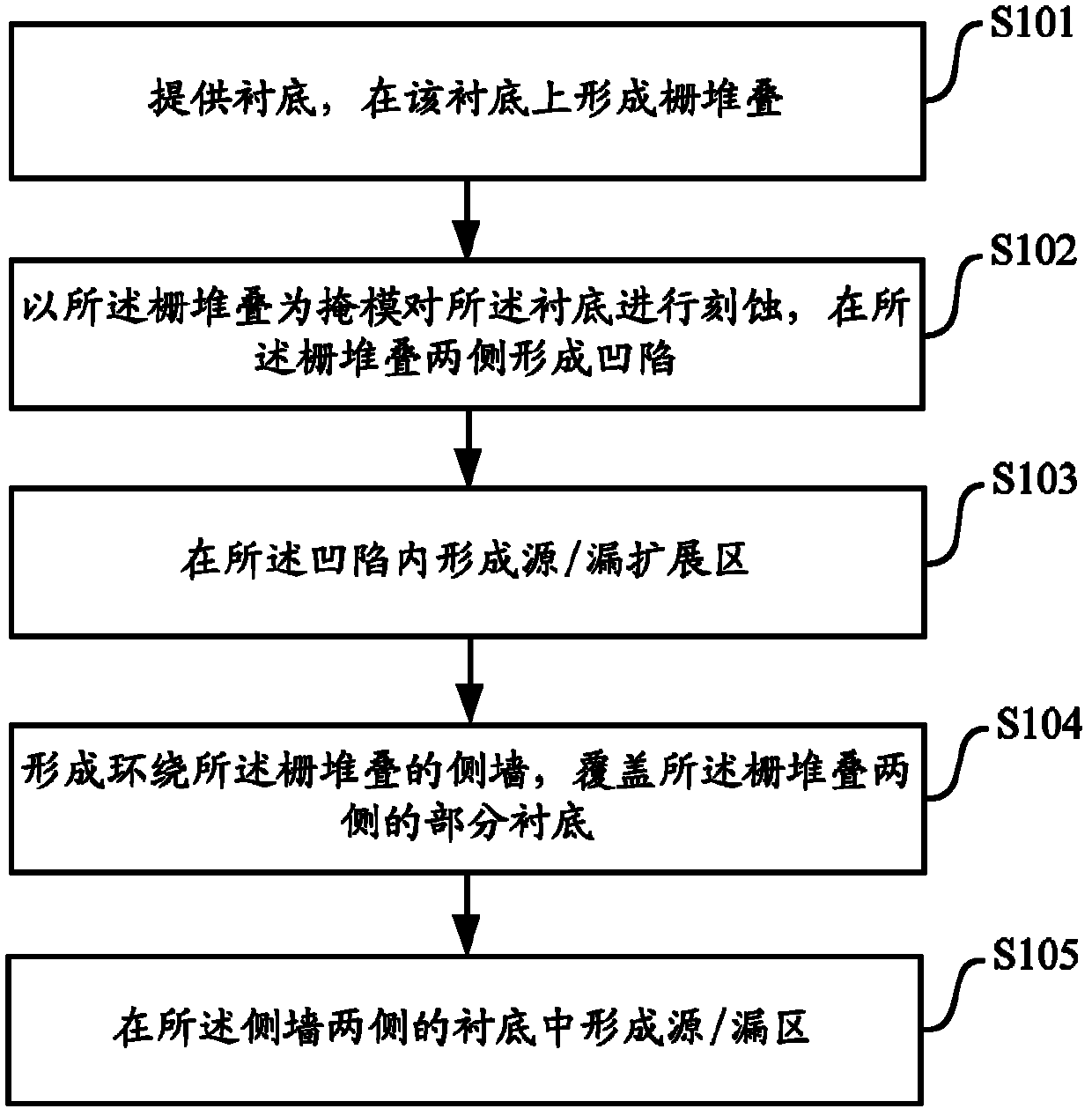
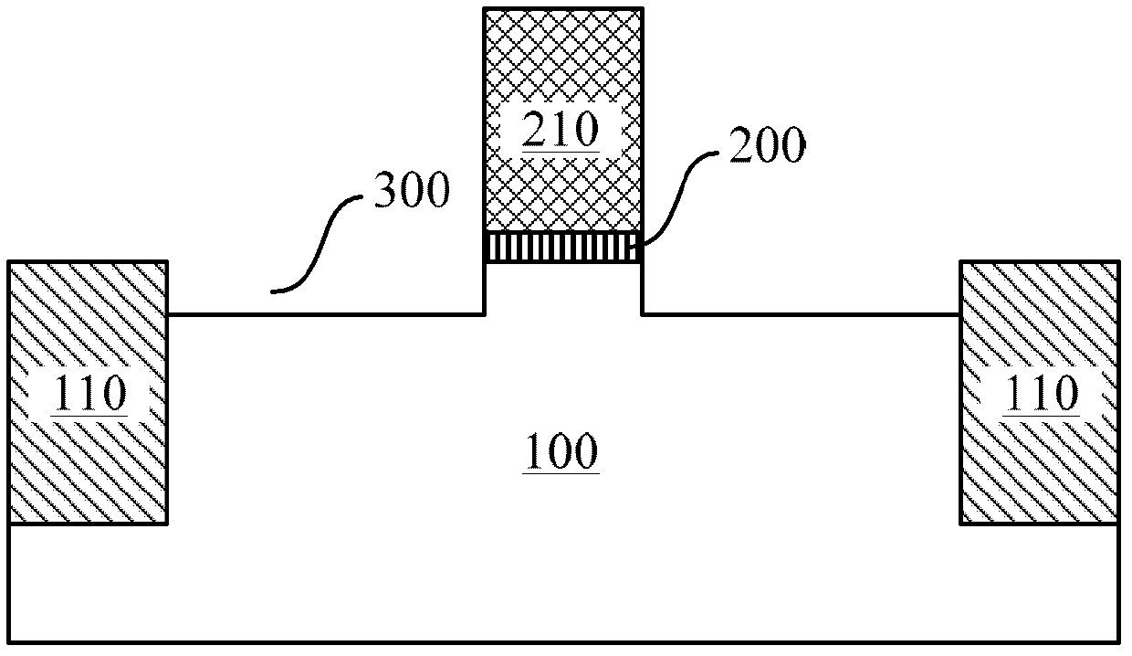
[0045] Embodiments of the present invention are described in detail below.

[0046] Examples of the described embodiments are shown in the drawings, wherein like or similar reference numerals designate like or similar elements or elements having the same or similar functions throughout. The embodiments described below by referring to the figures are exemplary only for explaining the present invention and should not be construed as limiting the present invention. The following disclosure provides many different embodiments or examples for implementing different structures of the present invention. To simplify the disclosure of the present invention, components and arrangements of specific examples are described below. Of course, they are only examples and are not intended to limit the invention. Furthermore, the present invention may repeat reference numerals and / or letters in different instances. This repetition is for the purpose of simplicity and clarity and does not in i...


PUM


Abstract

The invention provides a semiconductor structure which comprises a substrate, a grid stack arranged on the substrate, a side wall arranged on a side wall of the grid stack, a source / drain expansion zone arranged on the substrate on the two sides of the grid stack and formed in an epitaxial growth mode, and a source / drain zone arranged in the substrate on the two sides of the source / drain expansion zone. The invention further correspondingly provides a method for manufacturing the semiconductor structure. The semiconductor structure and the method for manufacturing the semiconductor structure can form the source / drain expansion zone which is high in doping concentration and small in depth so as to effectively improve performances of the semiconductor structure.

Description

technical field [0001] The invention relates to the technical field of semiconductors, in particular to a semiconductor structure and a manufacturing method thereof. Background technique [0002] The source / drain extension region (S / D junction extension) plays an important role in controlling the short channel effect of the MOS device and improving the driving capability of the device. [0003] The source / drain extension region is directly adjacent to the channel conduction region. As the gate length continues to decrease, the requirement for the junction depth of the source / drain extension region is also getting smaller and smaller, so as to suppress the increasingly serious short channel effect. However, the reduced junction depth of the source / drain extension region makes its resistance larger. If the series resistance of the source / drain extension region is not reduced in time, the parasitic resistance of the source / drain extension region will play a major role in the o...

Claims


Application Information

Patent Timeline
Patent Type & Authority Applications(China)
IPC IPC(8): H01L21/336H01L29/78
CPCH01L29/66636H01L29/7833H01L29/6653H01L29/66545H01L29/6656H01L29/66575
Inventor 殷华湘马小龙秦长亮徐秋霞陈大鹏
Owner INST OF MICROELECTRONICS CHINESE ACAD OF SCI
Why Eureka
Try Eureka