Light emitting diode and flip-chip light emitting diode package

一种发光二极管、封装组件的技术,应用在电气元件、半导体器件、电路等方向,能够解决减少发光二极管组件、热聚集、发光二极管发光面积减少等问题,达到电流分布均匀度提高、增加横向分布、提高发光效率的效果

Active Publication Date: 2013-09-11
NICHIA CORP
View PDF4 Cites 4 Cited by
  • Summary
  • Abstract
  • Description
  • Claims
  • Application Information

AI Technical Summary

Problems solved by technology

At least one groove is etched on the P-type semiconductor layer, and the groove extends to the N-type semiconductor layer, so that the N-type electrode is arranged on the N-type semiconductor layer. When the area of ​​the groove is smaller, the light-emitting area of ​​the light-emitting diode can be increased, but due to the N The contact area between the N-type electrode and the N-type semiconductor layer is too small, and the light-emitting diode is prone to heat accumulation when used at high current density.
Conversely, when the area of ​​the groove is larger, the light-emitting area of ​​the light-emitting diode is reduced, resulting in a decrease in the luminous efficiency of the light-emitting diode.
[0005] In view of the above problems, the present invention provides a light emitting diode component and a flip-chip light emitting diode packaging component, the light emitting diode component contacts the first type doped layer (N type semiconductor layer) by controlling the first contact (N type electrode) The area of ​​the LED is within an appropriate range, so that the LED component can be used at a high current density without the problem of heat accumulation, and will not reduce the light-emitting area of ​​the LED component and affect the luminous efficiency of the LED component

Method used


Image

  • Light emitting diode and flip-chip light emitting diode package
  • Light emitting diode and flip-chip light emitting diode package
  • Light emitting diode and flip-chip light emitting diode package

Examples


Embodiment Construction

[0076] In order to have a further understanding and understanding of the structural features of the present invention and the achieved effects, the preferred embodiments and accompanying drawings are used for a detailed description, as follows:

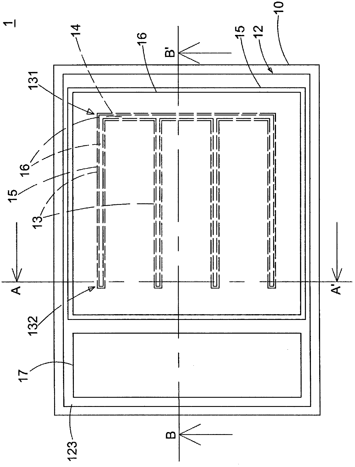
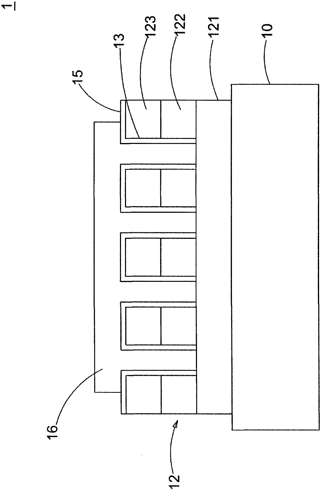
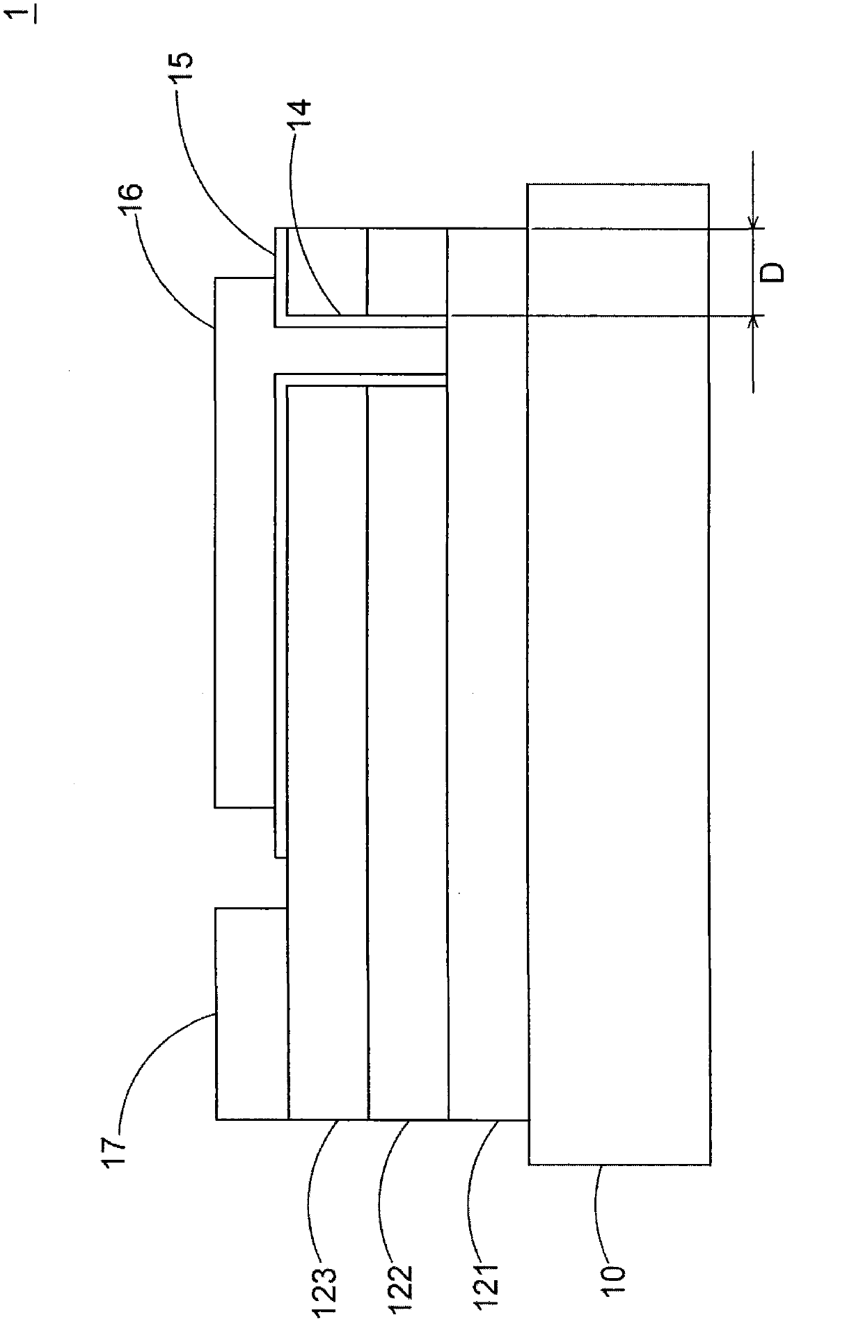
[0077] The present invention provides a light-emitting diode component, which includes: a component substrate; a first-type doped layer configured on the component substrate; a light-emitting layer configured on the first-type doped layer; a first-type doped layer The second-type doped layer, which is arranged on the light-emitting layer; a plurality of first grooves, which penetrate the second-type doped layer and the light-emitting layer and expose part of the surface of the first-type doped layer, each of which The first ditch has a first end and a second end; a second ditch is connected in series with the first ends of the first ditch, and the extending direction of the second ditch is different from that of the first ditch. The e...


PUM


Abstract

The invention provides a light emitting diode (LED) and a flip-chip light emitting diode package. The LED includes a substrate, a first-type doped layer, a light emitting layer, a second-type doped layer, a plurality of first grooves, a second groove, an insulation layer, a first contact, and a second contact. The LED is characterized in that the second groove is connected to one end of each first groove and penetrates the second-type doped layer and the light emitting layer to expose a part of the first-type doped layer. The contact area between the first contact and the first-type doped layer is increased. Therefore, the LED is worked at high current densities without heat accumulation. Moreover, the light emitting area is not reduced and the light emitting efficiency is not affected. The LED is flipped on a package substrate to form a flip-chip LED package.

Description

technical field [0001] The invention relates to a light-emitting diode component and a flip-chip light-emitting diode packaging component, in particular to a light-emitting diode component and a flip-chip light-emitting diode package that can be used for high current density. Background technique [0002] Electric energy is one of the indispensable energy sources today. For example, lighting devices, household electrical appliances, communication devices, transportation transmission, or industrial equipment, etc., cannot operate without electric energy. At present, most of the world's energy is burning oil or coal, but oil or coal is not inexhaustible. If we do not actively look for alternative energy sources, the world will fall into an energy crisis when oil or coal run out. In order to cope with the current energy crisis, in addition to actively developing various renewable energy sources, it is necessary to save energy and use energy effectively to improve the efficiency...

Claims


Application Information

Patent Timeline
Patent Type & Authority Applications(China)
IPC IPC(8): H01L33/14H01L33/20
CPCH01L33/14H01L33/38H01L33/382H01L33/36
Inventor 黄逸儒吴志凌罗玉云苏柏仁
Owner NICHIA CORP
Why Eureka
Try Eureka