Method for manufacturing ultra-thin ruthenium film by aid of plasma enhanced atomic layer deposition process

An atomic layer deposition and plasma technology, applied in metal material coating process, superimposed layer plating, semiconductor/solid-state device manufacturing, etc., can solve the problem of poor step coverage, diffusion barrier layer and seed crystal copper layer. Difficulty shrinking, shrinking semiconductor device feature size, etc., to avoid voids

Inactive Publication Date: 2013-09-11
FUDAN UNIV
View PDF4 Cites 0 Cited by
  • Summary
  • Abstract
  • Description
  • Claims
  • Application Information

AI Technical Summary

Problems solved by technology

[0003] However, with the further development of integrated circuit technology, the feature size of semiconductor devices continues to shrink. When the minimum feature size of integrated circuits gradually shrinks to 32 nanometers or below, this structure will face various challenges
With the large increase in the aspect ratio of trenches and vias, it is difficult to scale down the diffusion barrier layer and seed copper layer sputtered by physical vapor deposition (PVD), and the step coverage becomes poor, which may Can cause voiding in trenches and vias

Method used


Image

  • Method for manufacturing ultra-thin ruthenium film by aid of plasma enhanced atomic layer deposition process
  • Method for manufacturing ultra-thin ruthenium film by aid of plasma enhanced atomic layer deposition process
  • Method for manufacturing ultra-thin ruthenium film by aid of plasma enhanced atomic layer deposition process

Examples


Embodiment Construction

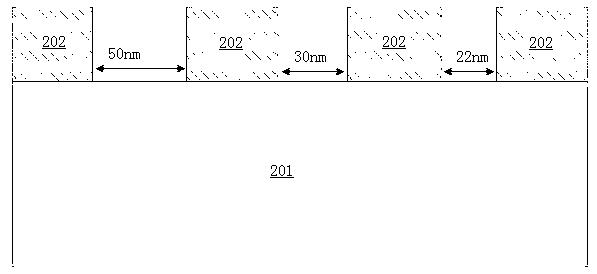
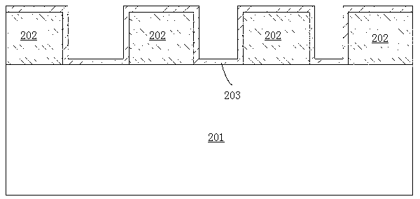
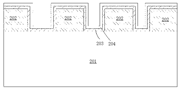
[0017] The method for preparing an ultra-thin ruthenium film by using a plasma-enhanced atomic layer deposition process proposed by the present invention includes: placing the substrate on which the ruthenium film needs to be grown into a reaction chamber, and heating the reaction chamber to 150° C. to 300° C., preferably Heating the reaction chamber to 250°C~270°C; then using the plasma-enhanced atomic layer deposition process to obtain a ruthenium film with a preset thickness by controlling the number of reaction cycles, wherein the ruthenium film is prepared by using the plasma-enhanced atomic layer deposition process A single reaction cycle consists of:

[0018] With bis (ethylcyclopentadienyl) ruthenium (II) (ie Ru (EtCp) 2 ) as the precursor, the Ru(EtCp) 2 Heating to 100°C~120°C, preferably Ru(EtCp) 2 Heat to 115°C and heat Ru(EtCp) 2 The obtained volatile gas is passed into the reaction chamber, and the passage time is 1 second to 10 seconds, and the preferred passa...


PUM


Abstract

The invention belongs to the technical field of copper interconnection processes for very-large-scale integrated circuits, and particularly relates to a method for manufacturing an ultra-thin ruthenium film by the aid of a plasma enhanced atomic layer deposition process. The method includes using double (ethyl cyclopentadienyl) ruthenium (II) as a precursor and adjusting the exposure time of oxygen plasmas to acquire pure ruthenium metal by the aid of the plasma enhanced atomic layer deposition process. The method has the advantages that the growth thickness of the ultra-thin ruthenium film can be precisely controlled in a nanometer scale by the aid of the plasma enhanced atomic layer deposition process, the ultra-thin ruthenium film is good in copper adhesiveness and excellent in copper insolubility during plating, trenches and through holes can be prevented from generating cavities, and seedless crystal copper plating can be implemented.

Description

technical field [0001] The invention belongs to the technical field of ultra-large-scale integrated circuit copper interconnection technology, and specifically relates to a method for preparing an ultra-thin ruthenium film by using a plasma-enhanced atomic layer deposition technology. Background technique [0002] In the copper interconnect technology of modern integrated circuits, an effective barrier layer must not only prevent copper from diffusing into the dielectric layer, but also improve the adhesion between the barrier layer and the dielectric layer. As we all know, in the 0.13 micron technology node, the tantalum / tantalum nitride (Ta / TaN) double-layer barrier layer has been successfully used in industrial copper interconnection technology. However, as the minimum feature size of integrated circuits is gradually reduced to 45 nanometers, the Ta / TaN double-layer barrier layer is facing many problems. For example, the proportional reduction of the barrier layer and the...

Claims


Application Information

Patent Timeline
IPC IPC(8): H01L21/768H01L21/283C23C28/00
Inventor 张春敏王鹏飞孙清清张卫
Owner FUDAN UNIV
Why Eureka
Try Eureka