Depletion mode MOS transistor and method of forming the same

A MOS transistor, depletion-mode technology, used in semiconductor devices, semiconductor/solid-state device manufacturing, electrical components, etc. On-state current and off-state current, the effect of increasing the equivalent resistance

Active Publication Date: 2016-12-28
SHANGHAI HUAHONG GRACE SEMICON MFG CORP
View PDF3 Cites 0 Cited by
  • Summary
  • Abstract
  • Description
  • Claims
  • Application Information

AI Technical Summary

Problems solved by technology

[0008] The technical problem to be solved by the present invention is to increase the off-state current of the transistor while increasing the switching current ratio of the depletion-type MOS transistor, resulting in an increase in the power consumption of the depletion-type MOS transistor

Method used


Image

  • Depletion mode MOS transistor and method of forming the same
  • Depletion mode MOS transistor and method of forming the same
  • Depletion mode MOS transistor and method of forming the same

Examples


Embodiment approach 1

[0042] Such as Figure 4 As shown, step S1 is firstly performed: providing a semiconductor substrate 100 with a well region 110 inside the substrate 100 .

[0043] The semiconductor substrate 100 may be a common substrate such as a bulk silicon substrate (bulk silicon), a silicon-on-insulator (SOI) substrate, or the like. The semiconductor substrate 100 has a well region 110 inside. In this embodiment, a depletion NMOS transistor is taken as an example, so the doping type of the well region 110 is P type.

[0044] In this embodiment, the method for forming the well region 110 includes: forming a patterned photoresist layer (not shown) on the semiconductor substrate 100, and performing ion implantation using the patterned photoresist layer as a mask to A well region 110 is formed in the substrate 100 . Wherein, in a specific embodiment, the process parameters of ion implantation to form the well region 110 include: the dopant ion is boron, and the implanted ion dose is 1E12 / c...

Embodiment approach 2

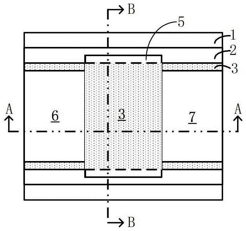
[0074] The shape of the doped region and the specific distribution of the doped region in the well region in the first embodiment are not limited to the above-mentioned embodiments, for example, in one example of the first embodiment, two doped regions are formed in the well region, In an example of the second embodiment, such as Figure 15 As shown, only one doped region 130 is formed on the surface of the well region. For another example, in another embodiment of the second embodiment, such as Figure 16 As shown, three doped regions 130 distributed at intervals are formed on the surface of the well region.


PUM


Abstract

The invention discloses a depleted MOS transistor and a forming method thereof. Part of a grid between a source and a drain covers well regions, and the other part of the grid covers doping regions, so that the equivalent resistance of a transistor channel is increased, and on-state and off-state currents of the depleted MOS transistor is reduced. Through adjustment of thicknesses and doping concentrations of the doping regions as well as the ratio of the sum of widths of all doping regions covered by the grid between the source and the drain to the width of the source or the drain in the transistor, the increasing quantity of the equivalent resistance of the transistor channel of the depleted MOS transistor can be kept moderate, therefore the reduction amplitude of the off-state current of the depleted MOS transistor is larger than that of the on-state current, and the on-off current ration of the depleted MOS transistor is improved while the power consumption of the transistor is reduced.

Description

technical field [0001] The invention belongs to the technical field of semiconductors, in particular to a depletion MOS transistor and a forming method thereof. Background technique [0002] According to the type of conductive channel (channel), MOS (metal-oxide-semiconductor) transistors can be divided into P-type MOS transistors and N-type MOS transistors; according to the relationship between channel and voltage, MOS transistors can be divided into enhancement MOS transistors ( enhanced MOS transistor) and depletion MOS transistor (depleted MOS transistor). When the voltage difference between the gate and source of the enhancement MOS transistor is zero, the enhancement MOS transistor cannot be turned on, so the enhancement MOS transistor can also be called a normally closed MOS transistor; when the depletion MOS transistor When the voltage difference between the gate and the source is zero, the depletion MOS transistor can be turned on, so the depletion MOS transistor c...

Claims


Application Information

Patent Timeline
Patent Type & Authority Patents(China)
IPC IPC(8): H01L21/336H01L21/28H01L29/78H01L29/423H01L29/06
Inventor 唐树澍
Owner SHANGHAI HUAHONG GRACE SEMICON MFG CORP
Why Eureka
Try Eureka