Photoelectromotive force device and manufacturing method thereof
A technology of photoelectromotive force and manufacturing method, applied in photovoltaic power generation, final product manufacturing, sustainable manufacturing/processing, etc., can solve the problems of low recombination speed, pollution adhesion, fixation, etc., and achieve the prevention of open circuit voltage (Voc, photoelectric conversion efficiency Efficiency effect
- Summary
- Abstract
- Description
- Claims
- Application Information
AI Technical Summary
Problems solved by technology
Method used
Image
Examples
Embodiment approach 1
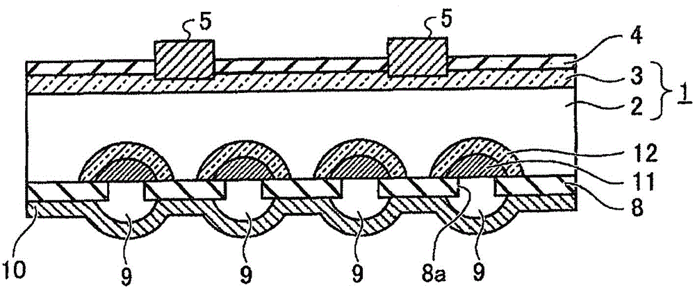
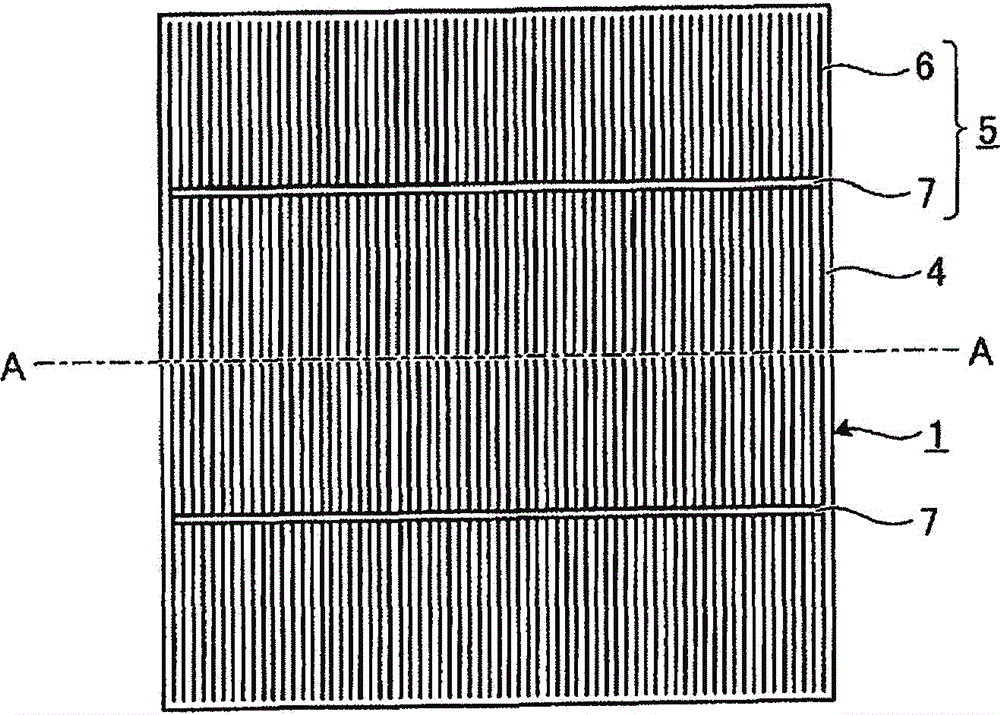
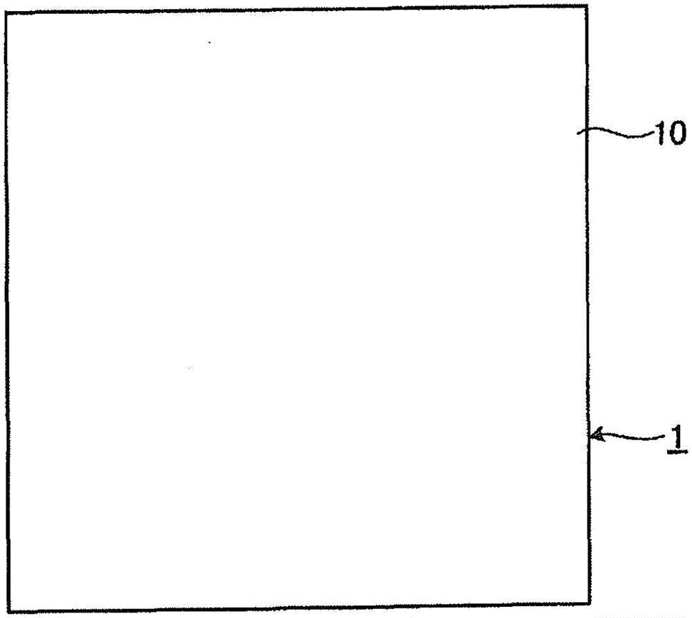
[0042] Figure 1-1 to Figure 1-3 It is a figure showing the structure of the solar battery cell which is the photovoltaic device of this embodiment, Picture 1-1 It is a sectional view of main parts for explaining the sectional structure of a solar battery cell, Figure 1-2is a plan view of the solar battery cell viewed from the light-receiving surface side, Figure 1-3 It is a bottom view of the solar battery cell viewed from the side (back side) opposite to the light receiving surface. Picture 1-1 yes Figure 1-2 Sectional view of the main part of the line segment A-A.
[0043] The solar cell unit of this embodiment is such as Figure 1-1 to Figure 1-3 As shown, it is equipped with: a semiconductor substrate 1, which is a solar cell substrate having a photoelectric conversion function and has a pn junction; an antireflection film 4, which is formed on the surface (surface) of the light-receiving surface side of the semiconductor substrate 1, and is used as an antireflecti...
Embodiment approach 2
[0101] In Embodiment 2, as another form of the back reflection film 10 , a case where the back reflection film 10 is formed of a metal foil will be described. Figure 7 is a sectional view of main parts for explaining the sectional structure of the solar battery cell according to this embodiment, and is the same as Picture 1-1 corresponding figure. The solar cell according to Embodiment 2 differs from the solar cell according to Embodiment 1 in that the back reflective film is not a silver sputtered film but is made of aluminum foil (aluminum sheet). The other structures are the same as those of the solar battery cell according to Embodiment 1, and thus detailed description thereof will be omitted.
[0102] Such as Figure 7 As shown, in the solar battery cell of this embodiment, the conductive adhesive 21 arranged on the back aluminum electrode 9 is attached to the back surface of the semiconductor substrate 1 so as to cover the back aluminum electrode 9 and the back insula...
Embodiment approach 3
[0115] In Embodiment 3, a rear surface structure will be described in which the solar battery cells of Embodiment 1 and Embodiment 2 include a metal sheet for connecting the cells when modularizing the solar battery cells. Electrodes for connection.
[0116] In recent years, in order to increase the efficiency of crystalline silicon solar cells, especially the suppression of the recombination speed on the rear surface has become more and more important. In both monocrystalline silicon solar cells and polycrystalline silicon solar cells, there are many cases where the carrier diffusion length exceeds the thickness of the silicon substrate. Therefore, the magnitude of the surface recombination velocity on the back surface of the silicon substrate greatly affects the characteristics of the solar cell.
[0117] On the other hand, when processing from a solar battery cell as a device unit to a solar battery module as an actual product, a plurality of solar battery cells are connec...
PUM
 Abstract
Description
Claims
Application Information
 - R&D
- Intellectual Property
- Life Sciences
- Materials
- Tech Scout
- Unparalleled Data Quality
- Higher Quality Content
- 60% Fewer Hallucinations
Browse by: Latest US Patents, China's latest patents, Technical Efficacy Thesaurus, Application Domain, Technology Topic, Popular Technical Reports.
© 2025 PatSnap. All rights reserved.Legal|Privacy policy|Modern Slavery Act Transparency Statement|Sitemap|About US| Contact US: help@patsnap.com


