
VCSEL (vertical cavity surface emitting laser) drive circuit

A vertical cavity surface and drive circuit technology, applied in the direction of lasers, laser components, semiconductor lasers, etc., can solve the problem of large inductance area on the chip, and achieve the effect of reducing the chip area and saving costs

Active Publication Date: 2013-06-26
SUZHOU LANGKUAN ELECTRONICS TECH
View PDF5 Cites 13 Cited by
  • Summary
  • Abstract
  • Description
  • Claims
  • Application Information

AI Technical Summary

Problems solved by technology

For the second circuit, each channel needs to use 4 on-chip inductors, and the number of 12-channel parallel channel inductors is as high as 48. Due to the large area of ​​on-chip inductors, considering the cost and chip area, this method is also not advisable.

Method used


Image

  • VCSEL (vertical cavity surface emitting laser) drive circuit
  • VCSEL (vertical cavity surface emitting laser) drive circuit
  • VCSEL (vertical cavity surface emitting laser) drive circuit

Examples


Embodiment 1

[0014] A common anode vertical cavity surface emitting laser (VCSEL) drive circuit, including an input buffer stage, a three-stage amplifier circuit, a current switch circuit and a bias current source circuit, the function of the input buffer is to realize impedance matching and adjust the operation of the circuit Level, resistors R1 and R2 are used to provide a suitable working level, and resistors R3 and R4 provide input impedance matching; the three-stage amplification structure adopts a cascaded full differential amplification structure with low load impedance to amplify the input signal and provide Sufficient gain, so that within a given range of input signal amplitude, sufficient voltage swing can be obtained on the current switch tube to promote the effective operation of the current switch; in this embodiment, the modulation current is directly coupled to the cathode of the VCSEL, and the bias current source passes through The off-chip inductor is DC-coupled to the cath...

Embodiment 2

[0016] A common cathode vertical cavity surface emitting laser (VCSEL) driving circuit, such as Figure 4 As shown, it includes an input buffer stage, a three-stage amplifier circuit, a current switch circuit and a bias current source circuit. The function of the input buffer is to achieve impedance matching and adjust the working level of the circuit. Resistors R1 and R2 are used to provide suitable Working level, resistors R3 and R4 provide input impedance matching; the three-stage amplification structure adopts a cascaded full differential amplification structure with low load impedance to amplify the input signal and provide sufficient gain, so that at a given input signal amplitude Within the range, sufficient voltage swing can be obtained on the current switch tube to promote the effective operation of the current switch; the output signal of this embodiment is AC-coupled to the common-cathode VCSEL anode through the capacitor (C1), and the VCSEL anode voltage is provided...


PUM


Abstract

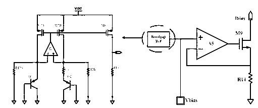
The invention discloses a VCSEL (vertical cavity surface emitting laser) drive circuit used for supplying sufficient drive current and voltage to a VCSEL. The VCSEL drive circuit comprises an input buffer, a three-stage amplifier circuit, a current switch circuit and a bias current source circuit. The input buffer is used for impedance matching and adjustment of operating level of the circuit. The three-stage amplifier circuit is used for amplifying input signals, and providing sufficient gain to allow the current switch tube to obtain sufficient voltage swing in a given input signal amplitude range so as to push a current switch to effectively operate. A bias current source is DC-coupled to a cathode of the VCSEL through an off-chip inductor and provides proper direct bias current for the VCSEL, the effect of output alternating current on bias current can be reduced, and photoelectric conversion efficiency of the VCSEL is maximized. One differential output end of the current switch is connected with a power source, and the other differential output end of the current switch is connected to the cathode of the VCSEL. The magnitude of modulation current can be controlled by adjusting Vmod end voltage. The magnitude of direct bias current can also meet requirements of different VCSEL tube threshold currents by adjusting Vbias end voltage.

Description

technical field [0001] The invention is used in an optical transmitter of an optical communication system to realize the function of driving a vertical cavity surface emitting laser, and belongs to the technical field of optical communication devices. Background technique [0002] The International Technology Roadmap for Semiconductors (ITRS) points out that the growth rate of chip performance has far exceeded the growth rate of interconnect performance. The traditional electrical interconnection between chips has problems such as limited bandwidth, serious crosstalk, and high power consumption, and cannot meet the system application requirements of large-capacity data transmission, new-generation communication equipment, and high-performance computers. As a new interconnection method, optical interconnection has many incomparable advantages of electrical interconnection, such as high bandwidth, low power consumption, small delay, and anti-interference. At present, the band...

Claims


Application Information

Patent Timeline
Patent Type & Authority Applications(China)
IPC IPC(8): H01S5/042
Inventor 李奚鹏
Owner SUZHOU LANGKUAN ELECTRONICS TECH
Learn More