Vertical-structure LED (light emitting diode) production method utilizing multi-layer dielectric film reflection

A technology of light-emitting diodes and multi-layer dielectrics, applied in electrical components, circuits, semiconductor devices, etc., can solve the problems of affecting reflectivity, affecting light-extraction efficiency of light-emitting diodes, poor adhesion, etc.

Inactive Publication Date: 2013-06-05
TONGFANG OPTO ELECTRONICS
View PDF4 Cites 6 Cited by
  • Summary
  • Abstract
  • Description
  • Claims
  • Application Information

AI Technical Summary

Problems solved by technology

At present, in the production of GaN-based vertical structure light-emitting diodes, the p-type ohmic contact mostly uses metals with high reflectivity, such as Ag, but it is well known that Ag has poor adhesion, so an adhesion layer must be pre-plated before Ag plating. However, due to the introduction of the adhesion layer, the reflectivity will inevitably be reduced. On the other hand, as the temperature rises, the metal diffusion will intensify, and the metal diffusion will inevitably affect the reflectivity, thereby affecting the light extraction efficiency of the LED.

Method used


Image

  • Vertical-structure LED (light emitting diode) production method utilizing multi-layer dielectric film reflection
  • Vertical-structure LED (light emitting diode) production method utilizing multi-layer dielectric film reflection
  • Vertical-structure LED (light emitting diode) production method utilizing multi-layer dielectric film reflection

Examples


Embodiment Construction

[0023] The preparation steps of the inventive method are as follows:

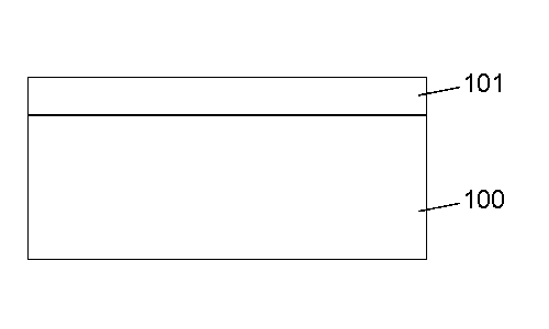
[0024] ① First, if figure 1 As shown, a GaN-based epitaxial layer 101 is heteroepitaxially grown on a sapphire substrate 100, and the GaN-based epitaxial layer 101 sequentially includes an n-type GaN-based semiconductor layer, an active layer and a p-type GaN-based semiconductor layer from bottom to top.

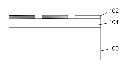
[0025] ② if figure 2 As shown, the electron beam evaporation method is used to deposit a multilayer dielectric film 102 on the GaN-based epitaxial layer 101. The multilayer dielectric film 102 is made of SiO2 and TiO2, and the thicknesses are 75nm and 40nm respectively. The etching process exposes part of the surface of the p-type GaN semiconductor layer as a conductive channel.

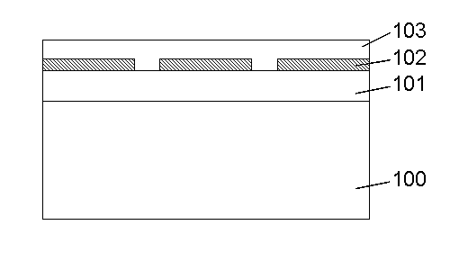
[0026] ③ if image 3 As shown, the ohmic contact metal layer 103 is deposited on the surface of the multilayer dielectric film 102 and the exposed part of the p-type GaN semiconductor layer by electron beam evaporation meth...


PUM


Abstract

A vertical-structure LED production method utilizing multi-layer dielectric film reflection relates to semiconductor photoelectric devices. The method comprises the steps of firstly epitaxially growing a GaN-based (gallium nitride-based) epitaxial layer on a sapphire substrate; secondly, depositing multilayer dielectric films on the surface of a p-type GaN-based semiconductor layer, and removing the multilayer dielectric films on the partial region to reveal the surface of a p-type GaN semiconductor layer; thirdly, depositing an ohmic contact metal layer on the multilayer dielectric films and the upper surface of the revealed p-type GaN-based semiconductor layer; fourthly, depositing an electroplating seed layer on the upper surface of the ohmic contact metal layer; fifthly, forming a metal substrate on the upper surface of the electroplating seed player; sixthly, removing the sapphire substrate and reverting the device; seventhly, depositing a p-type electrode on an n-type GaN-based semiconductor layer; and eighthly, depositing an n-type electrode on the lower surface of the metal substrate. By utilizing the multilayer dielectric films to further improve the reflectivity of the p-type GaN ohmic contact layer of the vertical-structure LED, the light extraction efficiency of the GaN-based vertical-structure LED is effectively improved.

Description

technical field [0001] The invention relates to a semiconductor optoelectronic device, in particular to a method for manufacturing a vertical structure light-emitting diode that adopts multi-layer dielectric film reflection. Background technique [0002] Due to the advantages of low energy consumption, long life, light weight, and small size, light-emitting diodes have become more and more widely used. At present, light-emitting diodes are used in automotive interior and exterior lights, display backlights, outdoor landscape lighting, portable system flashlights, projector light sources, and advertisements. Light boxes, flashlights, traffic lights, etc. are widely used. Due to the low price of sapphire substrates and relatively mature technology, most GaN-based epitaxial growth still uses sapphire substrates as growth substrates. However, since sapphire is not conductive, most GaN-based light-emitting diodes adopt a lateral structure with electrodes on the same side. This ...

Claims


Application Information

Patent Timeline
Patent Type & Authority Applications(China)
IPC IPC(8): H01L33/00
Inventor 郭德博
Owner TONGFANG OPTO ELECTRONICS
Why Eureka
Try Eureka