
Dicing / die bonding integral film, dicing / die bonding integral film manufacturing method, and semiconductor chip manufacturing method

一种芯片焊接、半导体的技术,应用在半导体/固态器件制造、半导体器件、薄膜/薄片状的粘合剂等方向,能够解决半导体芯片控制膜厚困难等问题

Active Publication Date: 2013-05-15
RESONAC CORPORATION
View PDF8 Cites 9 Cited by
  • Summary
  • Abstract
  • Description
  • Claims
  • Application Information

AI Technical Summary

Problems solved by technology

However, when using a paste-like adhesive, there are problems such as extrusion of the adhesive from the semiconductor chip, oblique adhesion of the semiconductor chip, and difficulty in controlling the film thickness.

Method used


Image

  • Dicing / die bonding integral film, dicing / die bonding integral film manufacturing method, and semiconductor chip manufacturing method
  • Dicing / die bonding integral film, dicing / die bonding integral film manufacturing method, and semiconductor chip manufacturing method
  • Dicing / die bonding integral film, dicing / die bonding integral film manufacturing method, and semiconductor chip manufacturing method

Examples


Embodiment 1

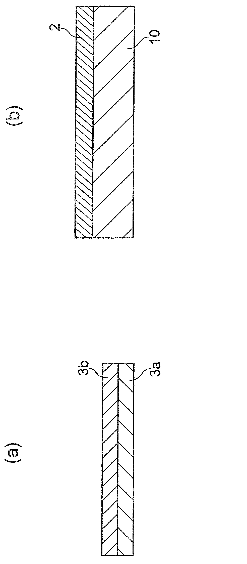
[0063] In Example 1, an example using a silicon wafer having a thickness of 75 μm and a diameter of 203 mm (8 inches) and a wafer ring having a diameter of 248 mm or more was shown. First, a 300-mm-wide dicing film (for example, SD-3001 Series manufactured by Hitachi Chemical Industries, Ltd.) in which an adhesive layer was formed on a base film was prepared. In addition, a die-bonding film (for example, FH-900 Series manufactured by Hitachi Chemical Industries, Ltd.) in which an adhesive layer was formed on a peelable base material was prepared.

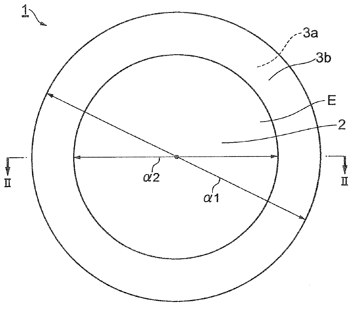
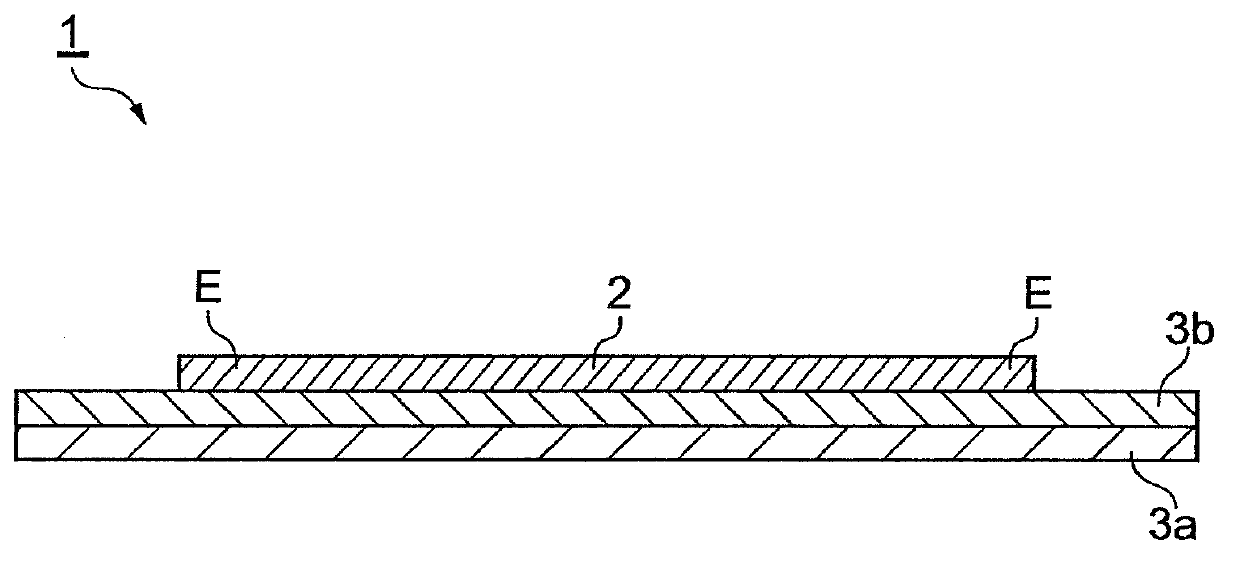
[0064] Next, the adhesive layer was pre-cut (pre-cut) so that the planar shape of the adhesive layer of the die-bonding film was a circle with a diameter of 223 mm. At this time, the adhesive layer is pre-diced so that the area of ​​the adhesive layer is larger than the area of ​​the silicon wafer to be diced and smaller than the area of ​​the adhesive layer and the base film.

[0065] Next, the surface on which the adhesive layer ...

Embodiment 2~8

[0068] In Examples 2-8, the diameters of the adhesive bond layer of the die-bonding film were 225 mm, 228 mm, 230 mm, 233 mm, 235 mm, 238 mm, and 240 mm, respectively, and the conditions were the same as in Example 1.

Embodiment 9~16

[0072] In Example 9, a silicon wafer with a thickness of 75 μm and a diameter of 305 mm (12 inches), a wafer ring with a diameter of 350 mm or more, and a dicing film with a width of 400 mm were used, and the diameters of the adhesive layer of the die-bonding film were 325 mm, 327 mm, and 330 mm, respectively. , 332mm, 335mm, 337mm, 340mm, 342mm, except that, it is the same condition as Example 1.


PUM

PropertyMeasurementUnit
diameteraaaaaaaaaa
diameteraaaaaaaaaa
diameteraaaaaaaaaa

Abstract

The disclosed dicing / die bonding integral film manufacturing method prevents the edge (E) of an adhesive layer (2) from peeling off of a pressure-sensitive adhesive layer (3b) during the process of dicing a semiconductor wafer (W). The disclosed dicing / die bonding integral film is provided with a substrate film (3a), a pressure-sensitive adhesive layer formed on the substrate film and bonded to a wafer ring (R) used in blade dicing, and an adhesive layer formed on the pressure-sensitive adhesive layer and having a central part bonded to the semiconductor wafer which is to be blade-diced, wherein the planar shape of the adhesive layer is circular, and the surface area of the adhesive layer is greater than that of the semiconductor wafer and smaller than that of the substrate film and that of the pressure-sensitive adhesive film. The diameter of the adhesive layer is greater than that of the semiconductor wafer and smaller than the inner diameter of the wafer ring. The difference between the adhesive layer diameter and the semiconductor wafer diameter is greater than 20mm and less than 35mm.

Description

technical field [0001] The present invention relates to a die bonding integrated film for blade dicing, a method for manufacturing the die bonding integrated film, and a method for manufacturing a semiconductor chip. Background technique [0002] Conventionally, a paste-like adhesive has been mainly used for bonding a semiconductor chip and a support member for the semiconductor chip. However, when a paste-like adhesive is used, there are problems such as extrusion of the adhesive from the semiconductor chip, oblique adhesion of the semiconductor chip, and difficulty in controlling the film thickness. [0003] In order to solve such a problem, in recent years, film adhesives instead of paste adhesives have attracted attention (for example, refer to the following patent documents 1 to 3). As a method of using the film-like adhesive, there is a method of sticking to the back of the wafer. In the method of sticking to the back surface of the wafer, first, after the film-like ...

Claims


Application Information

Patent Timeline
Patent Type & Authority Applications(China)
IPC IPC(8): H01L21/301H01L21/52C09J7/20
CPCH01L21/6836C09J7/0207H01L21/67092H01L2221/68377H01L2221/68327C09J2203/326C09J2201/606H01L21/67132C09J2201/61H01L21/78C09J7/02C09J2201/36C09J7/20Y10T156/1062Y10T428/21C09J2301/208C09J2301/304C09J2301/302H01L21/52H01L21/30
Inventor 加藤理绘松崎隆行加藤慎也古谷凉士作田龙弥小森田康二
Owner RESONAC CORPORATION
Learn More