Backside illuminated complementary metal-oxide-semiconductor transistor (CMOS) imaging sensor and preparation method thereof
An image sensor, back-illuminated technology, applied in the field of image sensors, can solve the problems of optical crosstalk, CMOS image sensor display fading, etc., to achieve the effect of eliminating phenomena, eliminating optical crosstalk, and avoiding optical crosstalk
- Summary
- Abstract
- Description
- Claims
- Application Information
AI Technical Summary
Problems solved by technology
Method used
Image
Examples
preparation example Construction
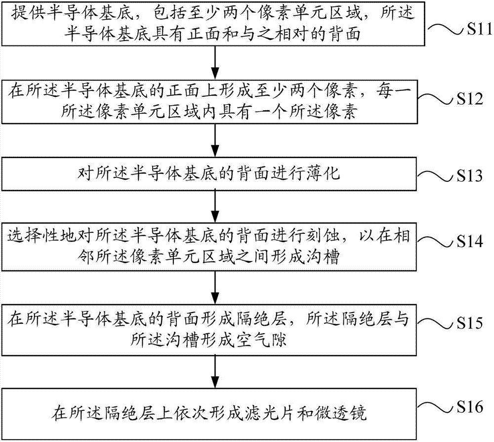
[0039] In combination with the above core idea, the present invention also provides a method for preparing a back-illuminated CMOS image sensor, including:
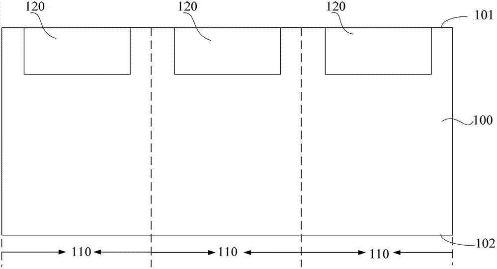
[0040] providing a semiconductor substrate comprising at least two pixel unit regions, the semiconductor substrate having a front surface and a back surface opposite thereto;
[0041] At least two pixels are formed on the front surface of the semiconductor substrate, each of the pixel unit areas has one of the pixels;
[0042] Thinning the back side of the semiconductor substrate;
[0043] selectively etching the back surface of the semiconductor substrate to form trenches between adjacent pixel unit regions;
[0044] formed on the back side of the semiconductor substrate, the isolation layer forms an air gap with the trench;
[0045]A filter and a micro lens are sequentially formed on the insulating layer.
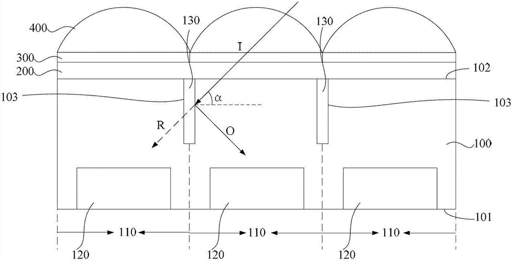
[0046] Please refer to the following figure 1 The back-illuminated CMOS image sensor of the present invention ...
PUM
 Abstract
Description
Claims
Application Information
 - R&D Engineer
- R&D Manager
- IP Professional
- Industry Leading Data Capabilities
- Powerful AI technology
- Patent DNA Extraction
Browse by: Latest US Patents, China's latest patents, Technical Efficacy Thesaurus, Application Domain, Technology Topic, Popular Technical Reports.
© 2024 PatSnap. All rights reserved.Legal|Privacy policy|Modern Slavery Act Transparency Statement|Sitemap|About US| Contact US: help@patsnap.com


