
Transparent conductive film, substrate with transparent conductive film, and organic electroluminescence element using same

一种透明导电膜、基材的技术,应用在电致发光光源、分散在不导电无机材料中的导电材料、导电材料等方向,能够解决损伤、无法透明导电膜103的表面导电性不均匀、导电性降低等问题

Inactive Publication Date: 2013-04-24
PANASONIC INTPROP MANAGEMENT CO LTD
View PDF5 Cites 12 Cited by
  • Summary
  • Abstract
  • Description
  • Claims
  • Application Information

AI Technical Summary

Problems solved by technology

In addition, the second transparent resin layer 106 may be damaged by the concave-convex first transparent resin layer 105.
In this way, when the materials of each transparent resin layer are mixed, or when one layer is damaged, there is a possibility that the conductivity will decrease or become uneven.
In addition, there is a possibility that the second transparent resin layer 106 cannot be evenly coated on the first transparent resin layer 105, resulting in uneven conductivity on the surface of the transparent conductive film 103.

Method used


Image

  • Transparent conductive film, substrate with transparent conductive film, and organic electroluminescence element using same
  • Transparent conductive film, substrate with transparent conductive film, and organic electroluminescence element using same
  • Transparent conductive film, substrate with transparent conductive film, and organic electroluminescence element using same

Examples


Embodiment 1)

[0069] As a substrate, non-alkali glass No. 1737 (refractive index of light with a wavelength of 500 nm: 1.50 to 1.53) manufactured by Corning Corporation was prepared. Next, on this base material, the material of the first transparent resin layer containing thin metal wires prepared in advance was applied to a thickness of 100 nm by the spin coating method, and heated at 100° C. for 5 minutes. Thus, the first transparent resin layer is formed on the base material. Next, the material for the first porous layer was applied on the first transparent resin layer so as to have a thickness of 30 nm, and heated at 100° C. for 5 minutes. Thus, a porous layer having a contact angle with water of 30 degrees was formed on the first transparent resin layer. Next, the material for the second transparent resin layer was applied on the porous layer so as to have a thickness of 100 nm, and heated at 100° C. for 5 minutes. Thus, the second transparent resin layer was formed on the porous lay...

Embodiment 2)

[0071] Instead of using the material for the first porous layer, the material for the second porous layer was used to form a second porous layer with a pore diameter of 10 nm and a contact angle with water of 60 degrees, except that it was produced and implemented in the same manner as in Example 1 above. Sample from Example 2.

Embodiment 3)

[0073] A sample of Example 3 was produced in the same manner as in Example 1 above except that the material for the first porous layer was coated on the substrate so as to have a thickness of 300 nm.


PUM

PropertyMeasurementUnit
aperture sizeaaaaaaaaaa
water contact angleaaaaaaaaaa
coating thicknessaaaaaaaaaa

Abstract

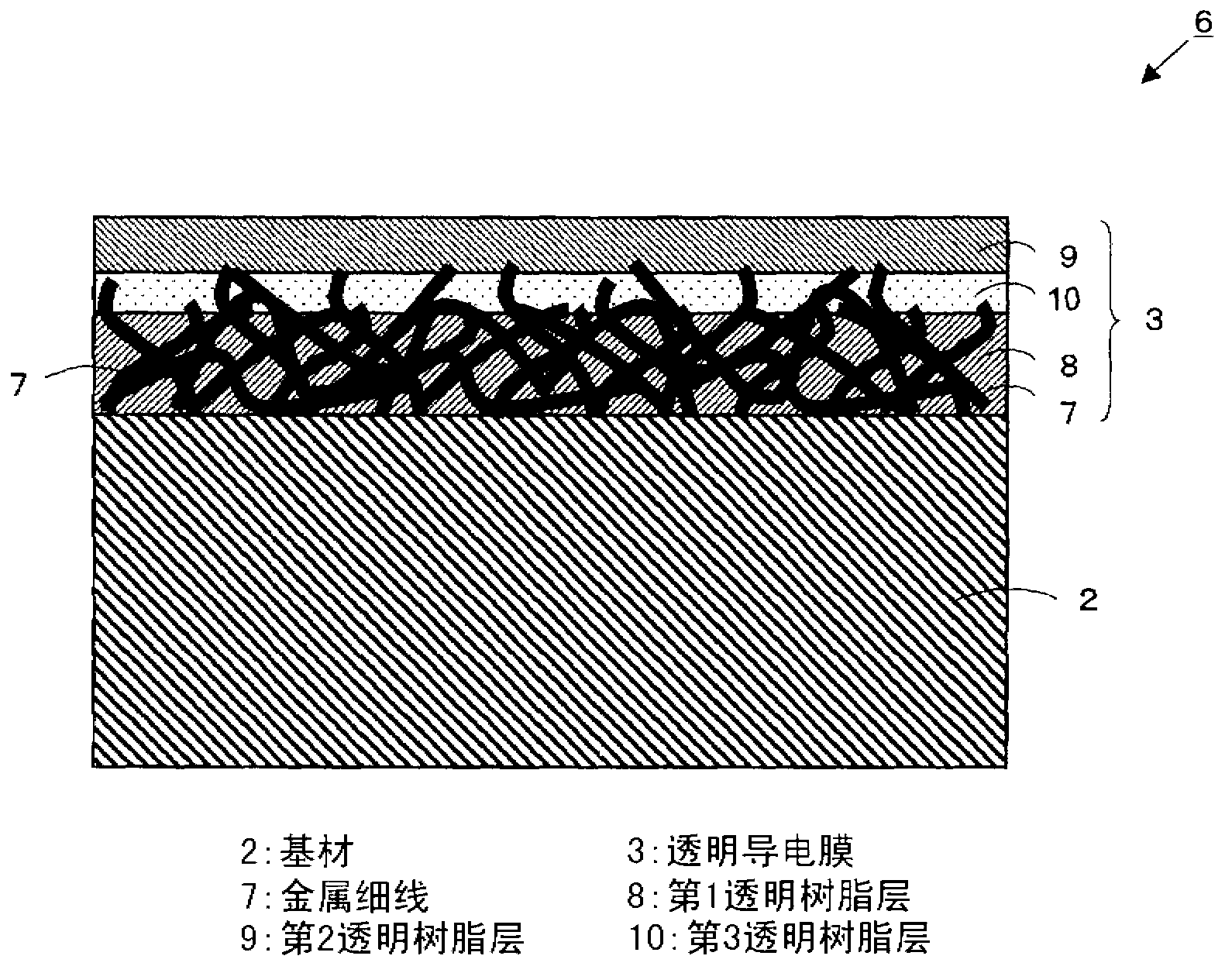
A transparent conductive film (3) comprises a first transparent resin layer (8) having a plurality of thin metallic wires (7), a second transparent resin layer (9) comprising a conductive polymeric molecule, and a third transparent resin layer (10) provided between the first transparent resin layer (8) and the second transparent resin layer (9). The second transparent resin layer (9) contains a water soluble resin, and the third transparent resin layer (10) contains a water insoluble resin or a water resistant resin. Because of the presence of the third transparent resin layer (10), the second transparent resin layer (9) can be prevented from mixing with the first transparent resin layer (8), and there is hardly any damage to the second transparent resin layer (9) by the first transparent resin layer (8). Accordingly, the surface of the second transparent resin layer (9) can be smooth and can have a uniform conductive property.

Description

technical field [0001] The present invention relates to a transparent conductive film used in various optical devices, a substrate with a transparent conductive film and an organic electroluminescent element using the same. Background technique [0002] A conventional organic electroluminescence (hereinafter referred to as organic EL) element is an element obtained by forming an organic light-emitting layer sandwiched by a pair of electrodes on a transparent substrate. side is extracted. In such an organic EL element, a material having conductivity and translucency is used as a material for the electrode on the substrate side, and indium tin oxide (hereinafter referred to as ITO) is widely used. However, electrodes using ITO as a material are fragile to bending and physical stress, and thus are fragile. In addition, in order to improve the conductivity of an electrode using ITO, a high vapor deposition temperature and / or a high annealing temperature are required, which may...

Claims


Application Information

Patent Timeline
Patent Type & Authority Applications(China)
IPC IPC(8): B32B27/18B32B27/00H01B5/14H01L51/50H05B33/02H05B33/28H10K99/00
CPCH01L51/5215H01L51/003H01B1/20H01B1/124H01B1/22Y10T428/265Y10T428/31678Y10T428/249979Y10T428/31663Y10T428/249986Y10T428/249991Y10T428/249993H10K71/80H10K50/816B32B27/08B32B27/20B32B2262/103B32B2262/106B32B2307/412B32B3/26B32B2457/20B32B2307/202
Inventor 辻本光松井太佑横川弘
Owner PANASONIC INTPROP MANAGEMENT CO LTD
Learn More