A method for preparing silicon nanowire arrays that are easy to separate in large areas
A silicon nanowire array, large-area technology, applied in nanomaterial technology and application fields, can solve the problem of destroying the order and integrity of silicon nanowire arrays, difficult to obtain uniform length silicon nanowire arrays, and affecting silicon nanowire arrays. Contact situation and other problems, to achieve the effect of weakened binding force, good repeatability and low cost
- Summary
- Abstract
- Description
- Claims
- Application Information
AI Technical Summary
Problems solved by technology
Method used
Image

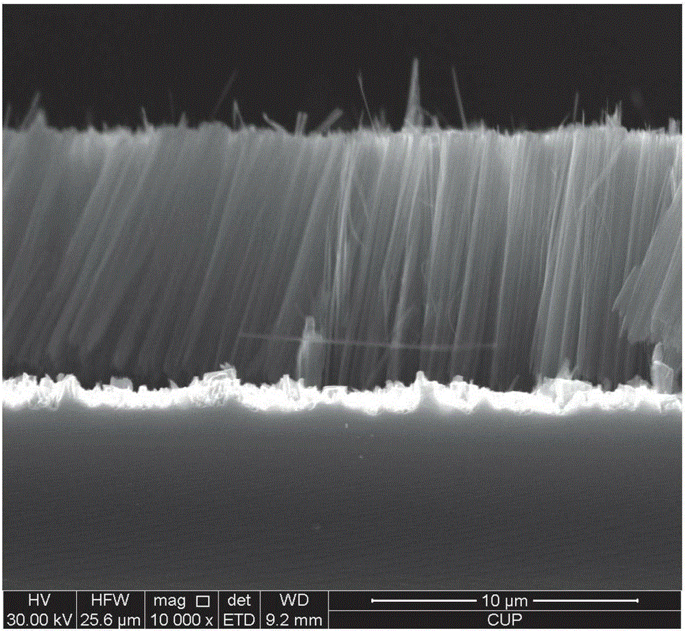
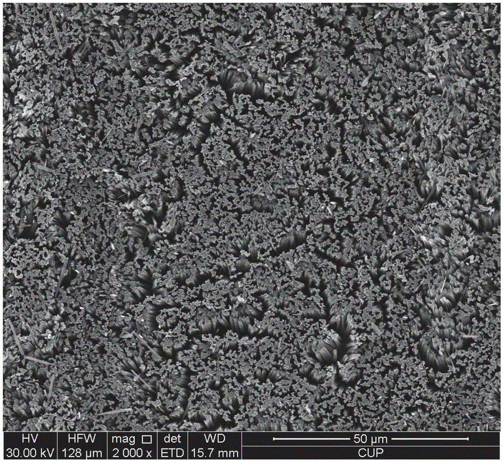
Examples
Embodiment 1
[0022] (1) Use a p-type (100) single chip with a resistivity of 7-13Ω·cm, ultrasonically clean it in acetone and absolute ethanol for 10 minutes, and then rinse it twice with ultra-pure deionized water; Soak in the solution at room temperature for 5 minutes; then soak in a hydrofluoric acid solution with a concentration of 14wt% for 5 minutes; soak and rinse in ultra-pure deionized water for 5 minutes, blow dry with nitrogen, and place in a vacuum drying environment;
[0023] (2) Connect two 7cm×7cm×3mm electrodes to the positive and negative poles of the constant current and voltage stabilized power supply respectively, fix their positions with an iron stand and keep the electrodes parallel, the electrode spacing is 1.5cm; then use a concentration of 4.6 ~5mol / L hydrofluoric acid and 0.01~0.02mol / L silver nitrate solution to prepare etching solution; preheat the etching solution to 25°C in a water bath;
[0024] (3) Fix the silicon wafer on a platform made of polytetrafluoroe...
PUM
| Property | Measurement | Unit |
|---|---|---|
| electrical resistivity | aaaaa | aaaaa |
| electrical resistivity | aaaaa | aaaaa |
Abstract
Description
Claims
Application Information
 - R&D
- Intellectual Property
- Life Sciences
- Materials
- Tech Scout
- Unparalleled Data Quality
- Higher Quality Content
- 60% Fewer Hallucinations
Browse by: Latest US Patents, China's latest patents, Technical Efficacy Thesaurus, Application Domain, Technology Topic, Popular Technical Reports.
© 2025 PatSnap. All rights reserved.Legal|Privacy policy|Modern Slavery Act Transparency Statement|Sitemap|About US| Contact US: help@patsnap.com