Point contact type diode

A diode and point contact technology, applied in the direction of electrical components, electric solid devices, circuits, etc., can solve the problem of poor forward and reverse characteristics of point contact diodes, no display of working parameters of point contact diodes, and inability to use large currents And rectification and other issues, to achieve the effect of cheap price, simple structure, convenient and correct use

Inactive Publication Date: 2013-04-10
孔明
View PDF0 Cites 4 Cited by
  • Summary
  • Abstract
  • Description
  • Claims
  • Application Information

AI Technical Summary

Problems solved by technology

However, compared with the surface junction type, the point contact type diode has poor forward and reverse characteristics, so it cannot be used for large current and rectification.
Point contact diodes are generally packaged in plastic shells, but the working parameters of point contact diodes are not displayed on the package, which is inconvenient to use

Method used


Image

  • Point contact type diode
  • Point contact type diode

Examples


Embodiment Construction

[0011] The present invention will now be further described in conjunction with specific examples, and the following examples are intended to illustrate the present invention rather than further limit the present invention.

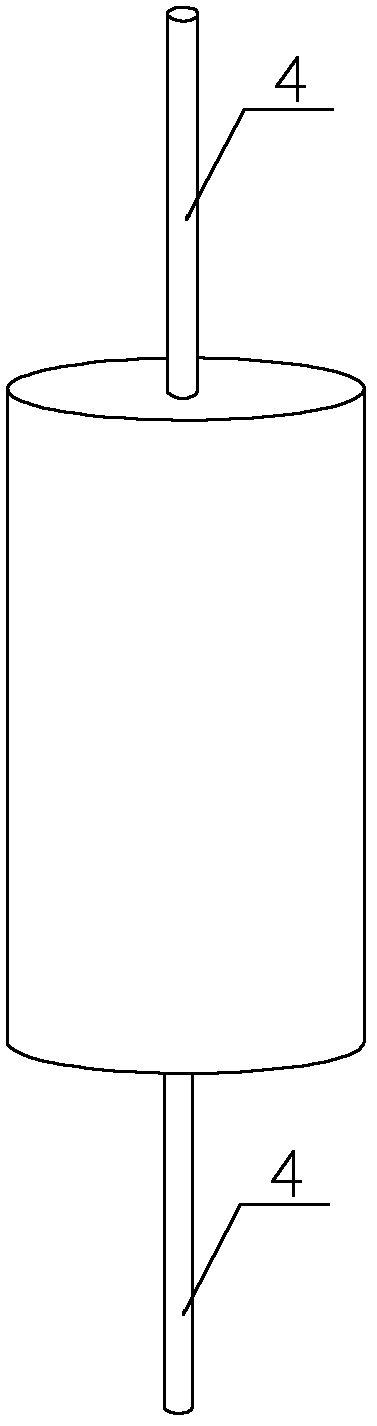
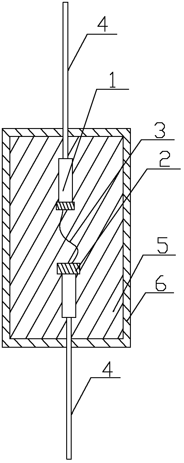
[0012] Such as Figure 1~2 The shown point-contact diode includes a diode body 1. The diode body 1 presses a contact wire 3 on a single chip 2, and a lead wire 4 is soldered to the other ends of the single chip 2 and the contact wire 3 respectively. Chip 2, contact wire 3, lead wire 4 welded with single chip 2 and contact wire 3 are partly plastic-sealed in epoxy resin tube 5, and epoxy resin tube 5 is coated with a layer that can clearly show the working parameters of diode body 1 Coating6.

[0013] The raw material of coating 6 is UV-curable ink, which can be cleaned by freon, alcohol, isopropanol and similar solvents, and the coating will not peel off.

[0014] Inspired by the above-mentioned ideal embodiment according to the present invention, throug...


PUM


Abstract

The invention relates to a semiconductor material, in particular to a point contact type diode which comprises a diode body. According to the diode body, a contact wire is pressed on a single chip, and two outgoing wires are welded to the single chip and the other end of the contact wire respectively. The single chip, the contact wire and the outgoing wires welded to the single chip and the contact wire are partially undergo plastic package in an epoxy resin pipe, and a layer of coating capable of clearly displaying working parameters of the diode body is coated outside the epoxy resin pipe. The point contact type diode is simple in structure, cheap in price and wide in applied range for general purposes such as small-signal detection, rectification, modulation, frequency mixing and amplitude limiting. The diode body undergoes plastic package in the epoxy resin pipe so as to guarantee that the electrical characteristics of the diode body are not influenced, the layer of coating capable of clearly displaying the working parameters of the diode body is coated outside the epoxy resin pipe, and the point contact type diode is convenient and correct to use.

Description

technical field [0001] The invention relates to a semiconductor material, in particular to a point contact type diode. Background technique [0002] Point-contact diodes are formed by pressing a metal needle on a single wafer and then using the current method. Therefore, the electrostatic capacitance of its PN junction is small, which is suitable for high frequency circuits. However, compared with the surface junction type, the point contact type diode has poor forward and reverse characteristics, so it cannot be used for large current and rectification. Point-contact diodes are generally packaged in a plastic case, but the working parameters of the point-contact diode are not displayed on the package, which is inconvenient to use. Contents of the invention [0003] The technical problem to be solved by the present invention is: based on the above problems, the present invention provides a point contact diode that can clearly display the working parameters. [0004] The...

Claims


Application Information

Patent Timeline
Patent Type & Authority Applications(China)
IPC IPC(8): H01L29/862H01L23/29H01L23/544
CPCH01L24/01
Inventor 孔明
Owner 孔明
Why Eureka
Try Eureka