Single-chip packaging piece with adhesive film replacing bottom fillers and manufacture process thereof

A manufacturing process and single-chip technology, applied in semiconductor/solid-state device manufacturing, electrical components, electrical solid-state devices, etc., can solve problems such as easy warpage and unguaranteed packaging reliability, achieve good protection of solder balls, reduce Possibility of wafer warpage, effect of reducing packaging cost

Inactive Publication Date: 2013-04-03
HUATIAN TECH XIAN
View PDF4 Cites 9 Cited by
  • Summary
  • Abstract
  • Description
  • Claims
  • Application Information

AI Technical Summary

Problems solved by technology

However, due to the limitations of traditional packaging in the past, the wafer can only be thinned to 200 μm, especially when the thickness is reduced to less than 100 μm, it is easy to warp, and the reliability of the package cannot be guaranteed.

Method used


Image

  • Single-chip packaging piece with adhesive film replacing bottom fillers and manufacture process thereof
  • Single-chip packaging piece with adhesive film replacing bottom fillers and manufacture process thereof
  • Single-chip packaging piece with adhesive film replacing bottom fillers and manufacture process thereof

Examples


Embodiment Construction

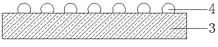
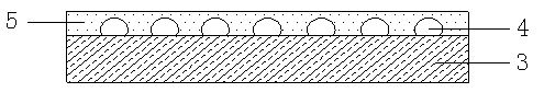
[0022] As shown in the figure, a single-chip package with an adhesive film instead of an underfill is mainly composed of a substrate 1, a nickel-gold pad 2, a chip 3, a tin-silver bump 4, an adhesive film 5, and a solder ball 8; The nickel-gold pad 2 is fixedly connected to the substrate 1, and the tin-silver bump 4 is fixedly connected to the chip 3; the tin-silver bump 4 coincides with the center line of the nickel-gold pad 2 and is connected by welding; the adhesive film 5 The gap between the substrate 1 and the chip 3 is filled, and the nickel-gold pad 2 and the tin-silver bump 4 are surrounded.

[0023] The chip 3 constitutes a circuit power supply and signal channel through tin-silver bumps 4 , nickel-gold pad 2 , substrate 1 and tin balls 8 .

[0024] As shown in the figure, a manufacturing process of a single-chip package with an adhesive film instead of an underfill is carried out in the following steps:

[0025] The first step, adhesive film 5: First, uniformly spin...


PUM


Abstract

The invention discloses a single-chip packaging piece with an adhesive film replacing bottom fillers and manufacture process thereof. The packaging piece is mainly composed of a substrate, a nickel pad, a chip, a solder silver bump, the adhesive film and a solder ball. The nickel pad is fixedly connected onto the substrate, and the solder silver bump is fixedly connected onto the chip; the solder silver bump is coincided with a central line of the nickel pad and connected with the central line of the nickel pad in soldering mode; and the adhesive film fills the gap between the substrate and the chip and surrounds the nickel pad and the solder silver bump. The manufacture process is conducted according to the following steps: pasting the adhesive film; installing the chip and reflow soldering; reducing thickness of the back of a wafer; and placing the ball, inspecting, packaging and putting in storage. By means of the technology, packaging cost is reduced, packaging reliability is improved, and process links are reduced.

Description

[0001] technical field [0002] The invention belongs to the technical field of integrated circuit packaging, and in particular relates to a single-chip package with an adhesive film instead of underfill and a manufacturing process thereof. Background technique [0003] Flip Chip technology is not only a chip interconnection technology, but also an ideal chip bonding technology. As early as 30 years ago, IBM has developed and used this technology. But until recent years, Flip-Chip has become a frequently used packaging form in the field of high-end devices and high-density packaging. Today, the application range of Flip-Chip packaging technology is becoming wider and wider, and the packaging forms are becoming more diversified, so the requirements for Flip-Chip packaging technology are also increasing. At the same time, Flip-Chip also poses a series of new serious challenges to manufacturers, providing reliable support for packaging, assembly and testing for this complex ...

Claims


Application Information

Patent Timeline
Patent Type & Authority Applications(China)
IPC IPC(8): H01L23/488H01L21/60
CPCH01L2924/15311H01L2224/16225H01L2224/32225H01L2224/73104H01L2224/73204H01L2924/18161H01L2924/00
Inventor 郭小伟刘建军谌世广崔梦刘卫东
Owner HUATIAN TECH XIAN
Why Eureka
Try Eureka