Method for manufacturing three-dimensional circuit

A manufacturing method and technology of three-dimensional circuits, applied in printed circuit manufacturing, circuits, printed circuits, etc., can solve problems such as insufficient circuit density, achieve good line size accuracy and conductor density, maintain stability, and have high material selectivity.

Inactive Publication Date: 2013-01-23
KUNSHAN LIANTAO ELECTRONICS CO LTD +1
View PDF5 Cites 16 Cited by
  • Summary
  • Abstract
  • Description
  • Claims
  • Application Information

AI Technical Summary

Problems solved by technology

However, when this problem is solved, it often leads to the disadvantage of insufficient circuit density

Method used


Image

  • Method for manufacturing three-dimensional circuit
  • Method for manufacturing three-dimensional circuit
  • Method for manufacturing three-dimensional circuit

Examples


Embodiment Construction

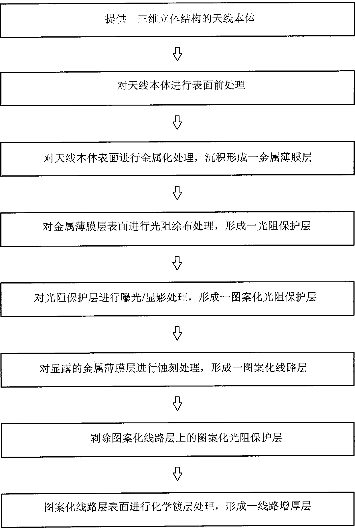
[0057] In order to further have a clear and detailed understanding and understanding of the structure, use and characteristics of the present invention, the preferred embodiments are now cited, and detailed descriptions are as follows in conjunction with the accompanying drawings:

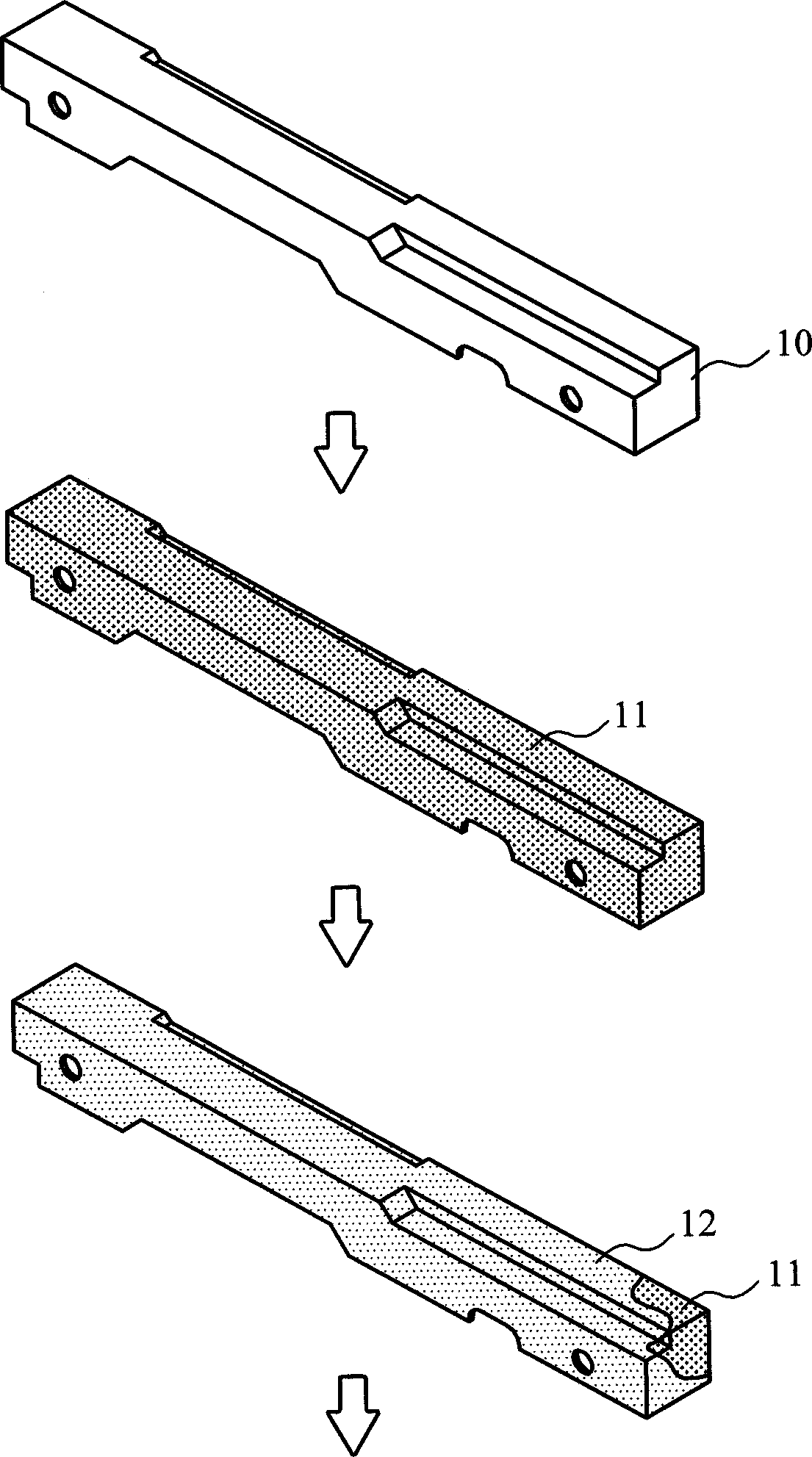
[0058] First, see figure 1 flow chart and Figure 2 to Figure 4 As shown in the structural diagram, in the first preferred embodiment, the manufacturing method of the three-dimensional antenna circuit of the present invention includes the following steps:

[0059] (1) An antenna body 10 with a three-dimensional structure is provided;

[0060] (2) carrying out surface pretreatment to antenna body 10;

[0061] (3) Carry out metallization treatment to the surface of the antenna body 10, deposit and form a metal thin film layer 11;

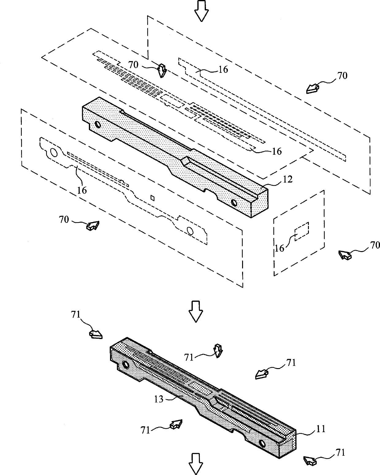
[0062] (4) Carry out photoresist coating treatment to the metal film layer 11 surface, form a photoresist protective layer 12;

[0063] (5) Exposing / developing 70 the ...


PUM


Abstract

The invention relates to a method for manufacturing a three-dimensional circuit. The method comprises the following steps of: providing a body with a three-dimensional structure; carrying out surface degreasing and roughening treatments on the body; carrying out metallization treatment on the body surface, and forming a metal film layer through precipitation; carrying out photoresist coating treatment on the surface of the metal film layer so as to form a photoresist protective layer; carrying out exposure / developing treatment on the photoresist protective layer so as to form a patterned photoresist protective layer; etching the exposed metal film layer so as to form a patterned line layer; removing the photoresist protective layer from the patterned line layer; and carrying out chemical plating treatment on the surface of the patterned line layer so as to form a line thickening layer. According to the method disclosed by the invention, a three-dimensionally wired circuit pattern can be directly formed on the body with the three-dimensional structure, and a circuit carrier is unnecessary to arrange on the body additionally, therefore the requirements of lightness, thinness, shortness and smallness are met.

Description

technical field [0001] The invention relates to a method for manufacturing a three-dimensional circuit, in particular to a method for forming a three-dimensional patterned metal circuit on the surface of a body of a three-dimensional structure. Background technique [0002] With the rapid development of today's wireless communication technology, related electronic communication products pay more and more attention to the quality of signal transmission and meet the needs of light, thin, short and small. However, various mobile image communication products (such as tablet computers, mobile phones, etc.) need to design different antenna body structures and circuit forms according to different product appearances and internal structure differences, so as to meet the miniaturization requirements of communication devices. [0003] In the known technology, laser direct structuring (LDS) is used to injection mold some special laser-activatable plastics into a predetermined body stru...

Claims


Application Information

Patent Timeline
Patent Type & Authority Applications(China)
IPC IPC(8): H05K3/00H05K3/06H05K3/38H01Q1/38H01L33/00
Inventor 胡泉凌陈誉尉
Owner KUNSHAN LIANTAO ELECTRONICS CO LTD
Why Eureka
Try Eureka