Grid voltage bootstrapped switch with low on-resistance and substrate bias effect elimination method thereof

A low on-resistance, gate voltage bootstrap technology, applied in the field of integrated circuits, can solve the problems such as the inability of M1 to be effectively turned off and the large on-resistance

Active Publication Date: 2013-01-23
TELINK SEMICON SHANGHAI
View PDF4 Cites 5 Cited by
  • Summary
  • Abstract
  • Description
  • Claims
  • Application Information

AI Technical Summary

Problems solved by technology

[0004] However, the turn-on voltage of the NMOS transistor is not only related to the voltage from the gate to the source, but also related to the voltage from the source to the substrate. The more the source is higher than the substrate voltage, the more obvious the lining bias effect is, and the threshold voltage is lower. The higher the value, the greater the on-resistance
In order to eliminate the background offset effect, the substrate and source terminals of M1 are usually shorted, but in figure 1 In the circuit, this will cause M1 to be unable to turn off effectively, because when the input signal is high, the input signal will conduct through the PN junction of the substrate and drain and the other end of the switch

Method used


Image

  • Grid voltage bootstrapped switch with low on-resistance and substrate bias effect elimination method thereof
  • Grid voltage bootstrapped switch with low on-resistance and substrate bias effect elimination method thereof
  • Grid voltage bootstrapped switch with low on-resistance and substrate bias effect elimination method thereof

Examples


Embodiment Construction

[0024] In order to make the objectives, technical solutions, and advantages of the present invention clearer, the various embodiments of the present invention will be described in detail below with reference to the accompanying drawings. However, a person of ordinary skill in the art can understand that, in each embodiment of the present invention, many technical details are proposed for the reader to better understand the present application. However, even without these technical details and various changes and modifications based on the following embodiments, the technical solutions claimed by the claims of this application can be realized.

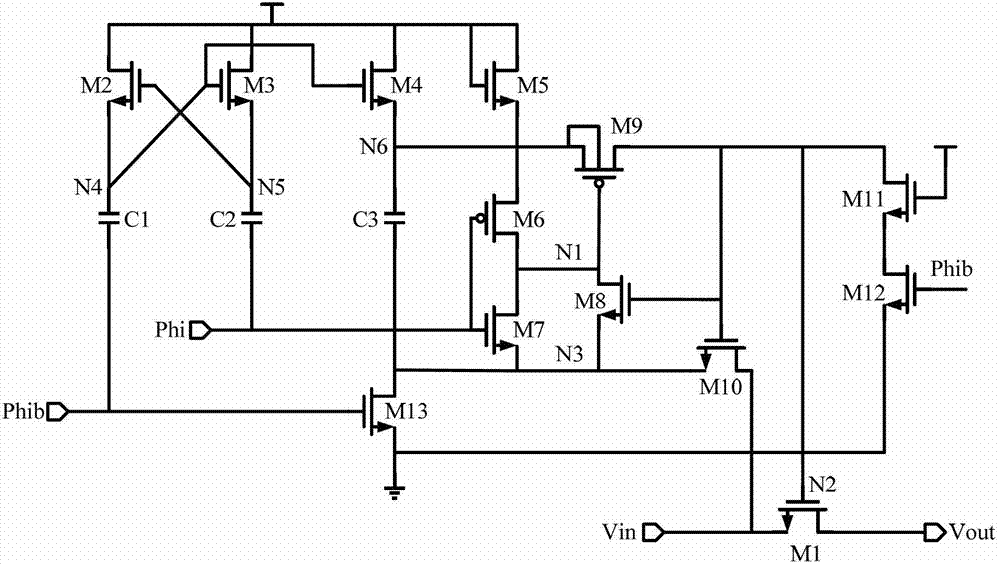
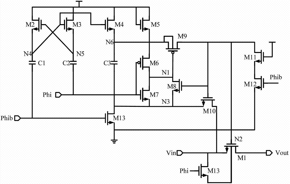
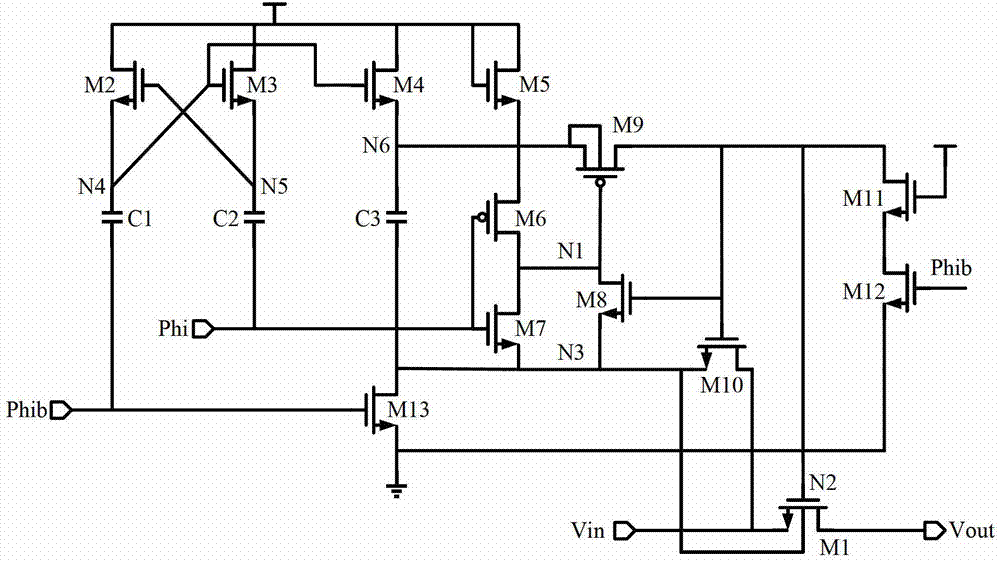
[0025] The first embodiment of the present invention relates to a gate voltage bootstrap switch with low on-resistance, including: a MOS transistor M1 as a switch, and a gate voltage bootstrap circuit connected to the MOS transistor M1. The gate voltage bootstrap circuit and the connection relationship between the gate voltage bootstrap ci...


PUM


Abstract

The invention relates to the field of integrated circuits and discloses a grid voltage bootstrapped switch with low on-resistance and a substrate bias effect elimination method thereof. According to the invention, a substrate of M1 which plays a switch role is not in direct short-circuiting with a source end of the M1 and is connected with the source end of the M1 through a control switch; when a grid voltage bootstrapped circuit is in a precharging mode, the control switch is at an turn-off state; and when the grid voltage bootstrapped circuit is in a bootstrapped mode, the control switch is at a turn-on state. Therefore, when the grid voltage bootstrapped circuit is in the precharging mode, the substrate of the M1 is grounded equivalently to ensure the thorough turn-off of the M1; and when the grid voltage bootstrapped switch is in the bootstrapped mode, the substrate of the M1 is communicated with a drain end of the M1 through the control switch, so that the substrate bias effect is eliminated, and the on-resistance of the switch M1 is kept unchanged no matter how many input signals are.

Description

Technical field [0001] The invention relates to the field of integrated circuits, and in particular to a technology for eliminating the offset effect of a gate voltage bootstrap switch. Background technique [0002] In analog circuits, MOS (metal oxide semiconductor) transistors are usually used to realize the switch function. Take the N-type MOS switch as an example. The on-resistance of the MOS tube is related to the voltage from the gate to the source. The smaller the voltage, the larger the on-resistance. Generally, when the switch is turned on, the gate voltage is fixed at a high level, and the source is connected to the input signal. Therefore, the on-resistance will change with the change of the input signal, especially when the signal voltage is close to the gate voltage, the N-type MOS transistor is approximately turned off. In order to process higher voltage signals, the gate is usually connected to the highest level, that is, the power supply voltage, provided that t...

Claims


Application Information

Patent Timeline
Patent Type & Authority Applications(China)
IPC IPC(8): H03K17/687
Inventor 谢循方飞
Owner TELINK SEMICON SHANGHAI
Why Eureka
Try Eureka