Method for promoting chip finished product rate through increasing standard cell through hole

A standard unit and yield technology, applied in electrical components, special data processing applications, instruments, etc., can solve problems affecting chip yield, open circuit defects, affecting chip functions, etc., to improve layout search efficiency, reduce defect probability, The effect of improving the yield rate

Inactive Publication Date: 2012-01-25
ZHEJIANG UNIV
View PDF0 Cites 0 Cited by
  • Summary
  • Abstract
  • Description
  • Claims
  • Application Information

AI Technical Summary

Problems solved by technology

[0002] In the integrated circuit manufacturing process, due to various uncertain reasons, there are defects in the through holes (Contact) in the chip production process, resulting in an abnormal increase in resistance and even open circuit defects.
The change of the electrical properties of the through hole will affect the function of the chip and affect the yield of the chip

Method used


Image

  • Method for promoting chip finished product rate through increasing standard cell through hole
  • Method for promoting chip finished product rate through increasing standard cell through hole
  • Method for promoting chip finished product rate through increasing standard cell through hole

Examples


Embodiment Construction

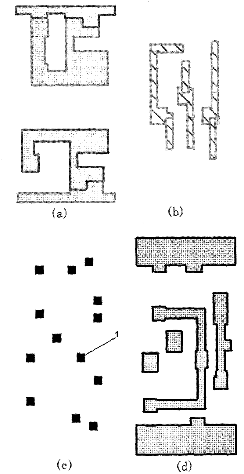
[0026] The present invention will be described below by taking the standard unit two-input AND gate as an example. The layout of the two-input AND gate is as follows figure 1 As shown, (a) is the layout of the active region (Active), (b) is the layout of the polysilicon layer (Poly), (c) is the layout of the contact layer, (d) is the layout of the metal layer . In this example, the via hole increase process starts with figure 1 The through hole marked with "1" in (c) is taken as an example.

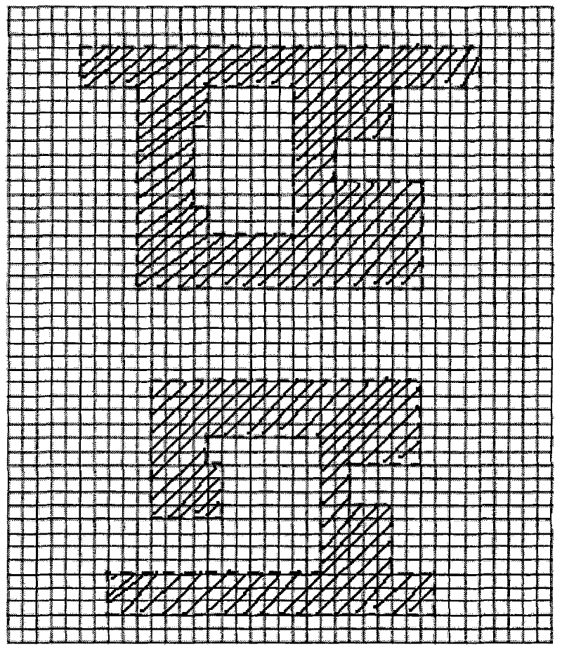
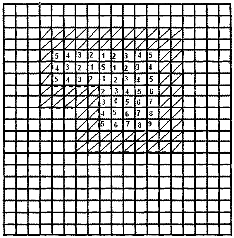
[0027] 1. After the chip design rules are integerized, the greatest common divisor λ of the design rules is obtained through the Stein algorithm cycle calculation; with λ as the basic unit, the layout of the standard cell polysilicon layer, active area layer, via layer and metal layer is evenly divided Form a rectangular grid, if there is no graphic on the grid point, set the grid point attribute to "0", and if there is a graphic on the grid point, set the grid point attribute to "1", ...


PUM


Abstract

The invention discloses a method for promoting chip finished product rate through increasing standard cell through holes. The method comprises the following steps: taking a greatest common divisor (lambada) regulated in chip design rules as a basic unit, evenly dividing a standard cell layout into rectangular grids, and setting grid point attribute structures and grid point attribute matrixes; through wave propagation operation and the and operation of the layout grid point attribute matrixes, dividing the through holes into through holes for connecting polysilicon and metals and through holes for connecting active regions and metals; conducting the wave propagation operations to the two kinds of through holes respectively at a through hole layer, a polysilicon layer, an active region layer and a metal layer, and conducting the and operations to the results of the wave propagation operations to obtain extensible subregions; and evenly increasing the through holes in the extensible subregions and modifying the layout grid point attribute matrixes to complete the increase of the standard cell through holes. On the premise that the area of the standard cell layout is unchanged, through increasing redundant through holes, the invention has the advantages that the probability of defects caused by through hole failure to standard cells is reduced, and the finished product rate of the standard cells can be obviously improved at low cost.

Description

technical field [0001] The invention relates to a method for increasing the yield of chips, in particular to a method for increasing the yield of chips by increasing through holes of standard units, and belongs to the field of integrated circuit design. Background technique [0002] In the integrated circuit manufacturing process, due to various uncertain reasons, there are defects in the through holes (Contact) in the chip production process, resulting in an abnormal increase in resistance, and even open circuit defects. The change of the electrical performance of the through hole will affect the function of the chip and affect the yield of the chip. [0003] Through-hole defects appear as random probability events. The reasons for random defects include: presence of photoresist impurities, voids caused by deposition, alignment errors of upper and lower layers, environmental impurity particles, chemical mechanical polishing (CMP) over-grinding, etc. These defects appear as...

Claims


Application Information

Patent Timeline
Patent Type & Authority Patents(China)
IPC IPC(8): G06F17/50H01L21/768
Inventor 罗小华严晓浪史峥郑勇军马铁中
Owner ZHEJIANG UNIV
Why Eureka
Try Eureka