Surface treatment device and method

A processing device and processing method technology, used in transportation and packaging, electrical components, semiconductor/solid-state device manufacturing, etc., can solve problems affecting the overall functionality of semiconductor components, pollution, and unusable range.

Inactive Publication Date: 2013-01-02
GALLANT PRECISION MACHINING CO LTD
View PDF5 Cites 2 Cited by
  • Summary
  • Abstract
  • Description
  • Claims
  • Application Information

AI Technical Summary

Problems solved by technology

[0003] In the wet etching process, one etching method is to immerse the silicon substrate in the etching solution, so that the etching solution simultaneously etches the upper and lower surfaces of the silicon substrate, and the other etching method is to etch a single surface of the silicon substrate. process, and does not treat the surface of the substrate other than the surface to be etched. In order to achieve this purpose, the etching solution can only touch the surface that is designated to be etched in the process. The overall functionality of semiconductor components may even lead to a part of the range that cannot be used and must be discarded. Therefore, when performing a single-sided etching process on a silicon substrate, how to effectively prevent the etchant from contaminating the non-designated etched surface has become the industry's constant concern. issue
[0004] In the prior art, there are many ways to prevent the non-designated etching surface from being contaminated with etching solution when etching a single surface of the silicon substrate. Some technologies are to add a protective layer (such as photoresist or glue) Designate the surface to be etched to avoid contamination of the etching solution in the process. However, this method requires an additional process of removing the protective layer after etching, which not only increases the complexity of the process, but also may cause residual glue if the removal is not complete. It is very inconvenient to cause contamination on the surface of the silicon substrate, or to scratch the substrate during the process of removing the protective layer

Method used


Image

  • Surface treatment device and method
  • Surface treatment device and method
  • Surface treatment device and method

Examples


Embodiment Construction

[0041] Since the present invention discloses a surface treatment device and method, the accompanying drawings below show the structural representations related to the features of the present invention, and are not and need not be completely drawn according to the actual size, and it is stated in advance.

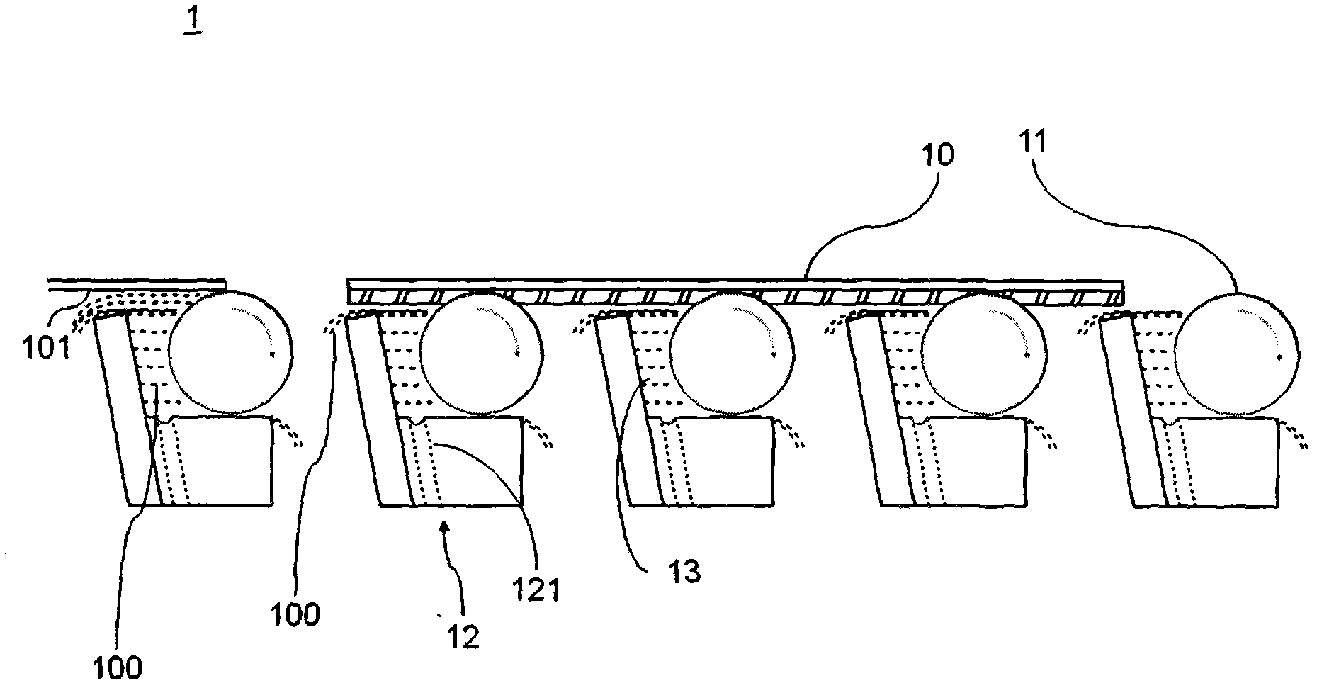
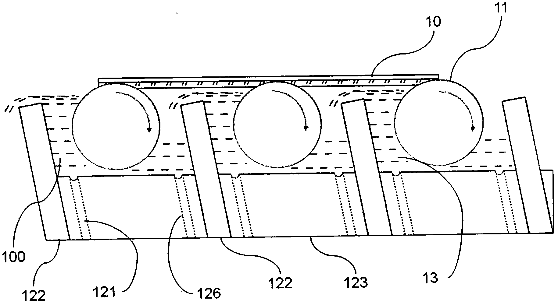
[0042] First please refer to figure 1 , The first embodiment of the present invention provides a substrate surface treatment device 1 , including a plurality of conveying devices 11 and at least one fountain seat 12 . The conveying device 11 can be used to convey the substrate 10, and the conveyed substrate 10 has a lower surface 101; the spring seats 12 are respectively arranged at intervals, and are respectively combined with the corresponding conveying device 11 to form the first liquid accumulation space 13, and each spring The seat 12 is provided with a liquid injection port 121, and each liquid injection port 121 communicates with its corresponding first liquid accumul...


PUM


Abstract

The invention provides a surface treatment device and a method. The surface treatment device comprises conveying devices and fountain bases. The conveying devices are used for conveying substrates, the fountain bases are assembled with the corresponding conveying devices respectively to form first liquid accumulation space, each fountain base is provided with a liquid injection port, the liquid injection ports are communicated with the corresponding first liquid accumulation space, the first liquid accumulation space can be used for accumulating a treating liquid injected by the liquid injection ports, the lower surfaces of the substrates conveyed by the conveying devices can be in contact with the treating liquid, and thereby the surface treatment process of the substrates can be performed.

Description

technical field [0001] The invention relates to a substrate surface processing device and method, in particular to a device and method for processing a single surface of a substrate. Background technique [0002] The application of semiconductor equipment in modern technology products is quite extensive, especially in electronic equipment such as communications, computers, networks, and optoelectronics, the existence of semiconductor silicon substrates is indispensable, and with the increasing market demand for these electronic products, How to quickly and efficiently improve the semiconductor production process and provide semiconductor components that meet the market demand is the goal of various manufacturers. In the general semiconductor production process, the process varies according to the design conditions required for the application of the silicon substrate. Among them is the wet chemical etching process. This wet process has a variety of technological applications...

Claims


Application Information

Patent Timeline
Patent Type & Authority Applications(China)
IPC IPC(8): H01L21/677H01L21/67H01L21/00
Inventor 张书省蔡嘉雄刘仕伟茹振宗
Owner GALLANT PRECISION MACHINING CO LTD
Why Eureka
Try Eureka