Graphene thin film transferring method based on physical adsorption

A graphene film and physical adsorption technology, applied in the field of materials, can solve the problems of complex transfer process, long transfer process, and unstable process, and achieve the effects of reducing environmental pollution, rapid transfer process, and avoiding glue residue

Active Publication Date: 2014-07-09
NANKAI UNIV
View PDF3 Cites 1 Cited by
  • Summary
  • Abstract
  • Description
  • Claims
  • Application Information

AI Technical Summary

Problems solved by technology

At present, the commonly used methods use thermal release glue and PMMA, but these methods have many glue residues, complicated transfer process, unstable process, and long transfer process, among which PMMA method is not suitable for large-area transfer.

Method used


Image

  • Graphene thin film transferring method based on physical adsorption
  • Graphene thin film transferring method based on physical adsorption
  • Graphene thin film transferring method based on physical adsorption

Examples


Embodiment 1

[0029] Transferring graphene on a metallic copper substrate to a 300nm thick SiO 2 layer on the Si wafer, including the following steps:

[0030] (1) Utilize the glass flake to process the copper foil with graphene thin film to be smooth;

[0031] (2) Attach the PET-silica gel layer to the copper foil;

[0032] (3) Put PET-silica gel / graphene / copper foil into FeCl with a concentration of 1mol / L 3 In the aqueous solution, soak for 1 hour to completely remove the metal copper and leave the PET-silica gel / graphene structure;

[0033] (4) Soak in 10% hydrochloric acid solution for half an hour, clean the PET-silica gel / graphene structure with deionized water, and dry it with nitrogen;

[0034] (5) Attach PET-silica gel / graphene structure to Si0 2 / Si chip;

[0035] (6) After sticking, lift the PET-silica gel layer to get SiO 2 / Si-based graphene.

[0036] figure 2 This is the optical microscopic image and atomic force scanning image after transfer. During the transfer pro...

Embodiment 2

[0038] Multiple use of PET-silica gel layers to transfer graphene on metallic copper substrates to SiO with a thickness of 300 nm 2 layer on the Si wafer,

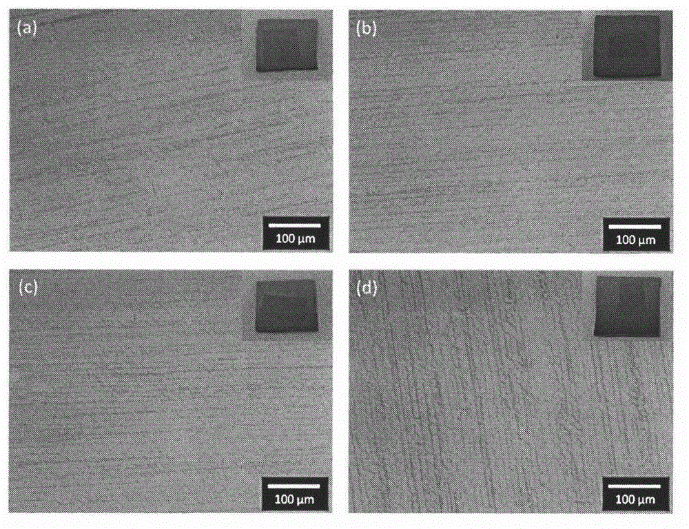
[0039] The specific steps are similar to Example 1, but after completing all the steps of Example 1 once, use the PET-silica gel layer peeled off in step (6) to continue to repeat the process of Example 1, so that it is repeated 4 times, that is, using a piece of PET -Silicone layer achieves 4 transfers, image 3 It is an optical microscopic image of the four transfer results, comparing the four results, and verifying that the multiple transfer of graphene can be achieved by using the PET-silica gel structure.

Embodiment 3

[0041] transfer graphene on metallic copper substrate to PDMS substrate,

[0042] The specific steps are similar to those in Example 1, but the target substrate used is a PDMS substrate.


PUM

PropertyMeasurementUnit
thicknessaaaaaaaaaa
thicknessaaaaaaaaaa
thicknessaaaaaaaaaa

Abstract

The invention relates to a graphene thin film transferring method based on physical adsorption, belonging to the technical field of materials, and relating to a method for transferring graphene to a flexible or rigid target substrate in large area and high quality. The method comprises the following steps of: firstly adhering a silica gel surface with a PET-silica gel structure onto a graphene/metal layer prepared by a chemical vapor deposition method; etching off a metal layer on the graphene thin film by utilizing a chemical etching liquid; tightly adhering the PET-silica gel/graphene structure onto the target substrate to be transferred; and peeling off a PET-silica gel layer to finish the transfer of the graphene to the target substrate. Through the method disclosed by the invention, the graphene thin film can be transferred to the flexible and rigid substrates in the large area and the high quality; without relating to an organic gel body, no gel is left after being transferred by utilizing the physical adsorption of the silica gel layer and the graphene; and in addition, the PET-silica gel layer can be reutilized so as to reduce the transfer cost and the environment pollution; and the graphene thin film transferring method based on the physical adsorption, disclosed by the invention, is suitable for large-scale application and production of the graphene thin films.

Description

technical field [0001] The invention relates to a graphene thin film transfer method, in particular to a transfer method for transferring graphene to a flexible or rigid substrate with high quality, large area and fast and simple based on physical adsorption, and belongs to the field of material technology. Background technique [0002] In 2004, two British scientists discovered that the carbon atom is formed by sp 2 A new type of two-dimensional atomic crystal-graphene (Graphene) composed of hybrid connected monoatomic layers. Since then, the research on graphene no longer stays at the theoretical stage. The basic structural unit of graphene is the most stable benzene six-membered ring in organic materials, and it is currently the most ideal two-dimensional nanomaterial. It consists of a dense layer of carbon atoms wrapped in a honeycomb crystal lattice, and is the thinnest two-dimensional material in the world, with a thickness of only 0.35nm. The strength of graphene is...

Claims


Application Information

Patent Timeline
Patent Type & Authority Patents(China)
IPC IPC(8): C01B31/04C01B32/184
Inventor 刘智波陈旭东田建国
Owner NANKAI UNIV
Why Eureka
Try Eureka